scispace - formally typeset
Search or ask a question
Journal ArticleDOI

3-D-DATE: A Circuit-Level Three-Dimensional DRAM Area, Timing, and Energy Model

01 Feb 2019-IEEE Transactions on Circuits and Systems I-regular Papers (Institute of Electrical and Electronics Engineers (IEEE))-Vol. 66, Iss: 2, pp 756-768
TL;DR: 3-D-DATE is presented, a circuit-level dynamic random access memory (DRAM) area, timing, and energy model that models both the front and back end of 3-D integrated DRAM designs from 90–16 nm, across a broader range of emerging transistor devices and through-silicon vias.
Abstract: In this paper, we present 3-D-DATE, a circuit-level dynamic random access memory (DRAM) area, timing, and energy model that models both the front and back end of 3-D integrated DRAM designs from 90–16 nm, across a broader range of emerging transistor devices and through-silicon vias. This paper improves upon previous studies by providing detailed process models all the way down to the 16-nm technology node and incorporating DRAMs implemented with emerging gate transistor devices. Finally, we validate the model against both several commodity planar and 3-D DRAMs, from 80- to 30-nm process nodes, with the following metrics: energy with a mean error of 5%–1% and a standard deviation up to 9.8%, speed with a mean error of 13%–27%, and a standard deviation up to 24% and area within 3%–1% and a standard a standard deviation up to 4.2%.

Summary (7 min read)

Introduction

  • A Circuit-Level Three-Dimensional DRAM Area, Timing, and Energy Model, also known as 3D-DATE.
  • A few studies have offered models for power and access latency calculations of DRAM designs in limited ranges.

1.1 Motivation

  • Three-dimensional die stacking involves connecting multiple silicon dies with a vertical interconnect, such as through-silicon vias (TSVs) or micro-bumps.
  • Three-dimensional die stacking reduces global wire routing inside of integrated circuits[1].
  • Samsung has shown that Wide-I/O has 330.6 mW read operating power in 50 nm process which is almost equal to LPDDR2 read power at the same process node.
  • Many studies have shown that 3D DRAM provides higher bandwidth with lower power consumption, as well as methods to utilize 3-D DRAM in memory hierarchies [2, 7–10].
  • Few studies have offered models for power and access latency calculations of custom designs.

1.2 Original Contributions

  • The goal of this work is to provide a 3D DRAM Area, Timing and Energy (DATE) model.
  • DATE not only can be used to model existing standard planar DRAM, but also for custom 3D DRAM designs or to find the optimal 3D DRAM design for architectures under exploration using traditional or emerging devices.
  • 2 DATE presents four different transistor models for modeling DRAM.
  • DATE demonstrates a new core design to support emerging VCAT based cell array layout as depicted in [11].
  • A more detailed comparison with other models are presented in Section 3.4.

1.4 Organization of Dissertation

  • Chapter 2 presents DRAM process node characterization.
  • Transistors, wires, and through silicon via (TSV) models, modeled from 90 nm to 16 nm technology nodes, are discussed.
  • Chapter 3 presents circuit-level model and architectural-level model of 3D DRAM.
  • Chapter 4 presents the first case study, which explores the benefits of 3D design space using a 1 Gb standard double-data-rate DRAM.

1.5 Abbreviations

  • ASC Asymmetric Channel Doping BL BitLine DATE DRAM Area, Timing, and Energy model DDR Double Data Rate DRAM Dynamic Random Access Memory F minimum Feature size FEOL Front-End-Of-Line FinFET Fin Field Effect Transistor 5 ITRS International Technology Roadmap for Semiconductors JEDEC Joint Electron Device Engineering Council LPDDR.
  • Low Power Double Data Rate MASTAR ITRS2005 roadmap provides partial information of gate transistor with wordline voltage from 80 nm node.
  • The roadmap does not provide any resistance and current information to calculate speed.
  • DATE presents DRAM roadmap from 90 nm technology node.

2.1 Transistor Model and Scaling

  • In DRAM, a gate transistor is required to reduce the leakage current and to retain the stored data in the cell capacitor during the required data retention time.
  • SRCAT provides more recessed channel effect than RCAT [23].
  • Thus, FinFET can be used as a gate transistor in a smaller technology node rather than a planar transistor [26, 29].
  • Vertical channel access transistor (VCAT) is another transistor that has been proposed as a bitcell transistor alternative for DRAMs [11, 24].
  • This allows for the bitcell transistor to be placed at the cross section of bitline and wordline and also allows VCAT dedicated denser cell layout such as 4 F 2.

2.1.1 Gate Transistor Model and Scaling

  • Their gate transistor roadmap is deployed with Synopsys Technology ComputerAided Design (TCAD) device simulator technology.
  • DATE provides roadmap from 90 nm for the comparison since vendors fabricate test chip in larger technology nodes [11].
  • Among these empirical data, RCAT threshold voltages are collected as shown 15 in Figure 2.5.

2.1.2 High-Voltage and Peripheral transistor

  • Peripheral and high voltage transistor roadmaps are deployed with a Model for Assessment of cmoS Technology And Roadmaps from ITRS [47].
  • Figure 2.6 shows the graphical user interface of MASTAR.
  • MASTAR has high performance (HP), low stand-by power (LSTP) and low operating power (LOP) process roadmaps with physical models of planar bulk, double gate (DG) and silicon on insulator (SOI) transistor.
  • From this assembly, the authors rely upon MASTAR process assumptions along with Rambus size projections.
  • DATE admits the ITRS projection for adjusting channel doping concentration.

2.2.1 Wire

  • For the wire resistance and wire capacitance calculation, DATE adopts Horowitz wire model [48].
  • For the general metal wire material, Horowitz and ITRS expected the technology would migrate from aluminum to copper because aluminum wires have a resistivity of 282 Ω·cm while copper wires have a resistivity of 170 Ω·cm at 20 ◦C [48–50].
  • In the technical report [51], DRAM uses a metal size similar to the global wire size of a microprocessor process.
  • There is a significant difference in the choice of inter-cell routing materials assumed between DATE and the technical report [51].
  • For the other metal layers, DATE adopts similar width sizes and aspect ratios from the cross-sectional report [51].

2.2.2 Through Silicon Via

  • TSVs are classified into different categories according to the fabricated order compared to the metal layer.
  • Figure 2.11 shows a top view of the FEOL TSV bundles along with coupled capacitance.
  • For the detailed calculation for each technology nodes, DATE follows CACT-3DD size roadmap for a conservative size scaling: ITRS provide size roadmap of TSVs.
  • DATE includes TSVs in the driving circuits.
  • The area calculations for TSVs includes the buffer chain unless the buffer chain can fit into the pitch of the TSV.

2.3.1 Gate Transistor

  • RCAT, SRCAT and VCAT have been simulated with Synopsys TCAD under the condition proposed in Table 2.1 and Figure 2.4.
  • Figure 2.13 shows three-dimensional view and cross-section of 27 28 VCAT TCAD simulation.
  • Both Rambus and CACTI-3DD assume similar capacitance scaling projection as shown in Figure 2.14.
  • Io f f below 5 fA with the lowest possible channel doping density while the threshold voltage met threshold voltage trend within the standard deviation (0.0665 V).

2.3.2 High Voltage and Peripheral Transistor

  • Table 2.5 shows capacitance and turn-on current roadmap of high-voltage (HV) transistors.
  • For the turn-on current, CACTI-3DD uses a fixed number on each node even through temperature changes.
  • DATE follows ITRS roadmap at 25 ◦C and reflects turn-on current change due to temperature changes based on MASTAR calculation.
  • Between CACTI-3DD and DATE, DATE exhibits more device capacitance because DATE adopts higher side-wall capacitance as discussed in the case of HV transistor and also expects more gate capacitance mainly due to longer channel length expectation of Rambus roadmap.
  • 2The Rambus and CACTI-3DD projection was derived and calculated based on the source code or data provided by the author.

2.3.3 Wire

  • Wire capacitance and resistance per µm have been calculated using the Horowitz equation for DATE.
  • The CACTI3DD roadmap is derived from the source code.
  • In M3 layer roadmap, DATE expects the smallest resistance in all nodes mainly due to it have the largest physical dimension compare to the ITRS and CACTI-3DD.
  • The normalized values of wire capacitance and resistance across three anonymous processes with those of DATE, ITRS, and CACTI-3DD, are presented in Table 2.8.
  • The anonymous processes are for the general logic design.

2.3.4 Through Silicon Via

  • Through silicon via (TSV) is mainly made by etching or laser drilling.
  • In DATE, the authors adopt CACTI-3DD TSV roadmap since they assume TSV size would scale due to technology advancement.
  • The Table 2.11 shows the DATE TSV roadmap calculated as described in Section 2.2.2.
  • Circuit level models can be expanded upon to calculate the resistance, capacitance, and area of the logic composed of multiple transistors.
  • Examples of circuit level modeling of the DRAM memory system are CACTI, CACTI-D, CACTI-3DD, and Rambus models introduced in Section 1.3.

3.1.1 General Layout and Drain Capacitance

  • In the circuit level model, the logic gate area, turn on resistance, and capacitance is derived from the physical geometry obtained from a transistor layout.
  • DATE assumes ideal layout design rules as shown in Figure 3.2 and Figure 3.3.
  • Only one of the two regions are considered.
  • The drain capacitance of the series-connected transistors is also calculated by adding all the capacitance shown in Figure 2.15 for the gray areas.

3.1.2 Digital Logic and Driving Buffer

  • DATE assumes that the buffer followed by the digital logic is driving the following logic or wire as shown in Figure 3.8.
  • Table 3.1 shows logical effort for inputs of logic gates.
  • For the driving buffer chain, Nils et al. [57] showed the optimum fanout of each inverter, that is, the optimum stage effort to achieve the least delay is within a range of 2.7 to 5.3 according to the technology dependency.
  • The transistor size for the logic in Figure 3.8 is decided by the number of inputs and also the kind of logic.
  • For the energy calculation of the gate, DATE accounts for drain-out charges by adding 56 capacitance of every node since the dissipated energy is given by the equation [55]: E =CL ×V 2×P0→1 (3.20) where CL is the sum of the intrinsic capacitance of the gate and loaded capacitance of the output.

3.1.3 Repeater for Wire

  • When wire length linearly increases, the delay of wire increases quadratically since both resistance and capacitance increase linearly.
  • Also, large wire load on the driver leads to excessive short-circuit power dissipation on the last stage of the driver, which is due to the degrading of the waveform shape [60].
  • The general design approach is to introduce a repeater to resolve the problems caused by large wire loads.
  • In the DATE model, Rabaey’s approach is adopted for the repeater model [55].
  • Γ stands for the ratio of input capacitance and output capacitance of a minimum size inverter.

3.1.4 Address Decoder

  • DATE provides a two-stage address decoder for both row and column address decoding as shown in CACTI5.1 [62] and described in Rambus model [13].
  • After the MWL, there is a sub-wordline (SWL) which is driven by the inverter buffer.
  • The row address path consists of the predecoder stage and following second stage decoder blocks.
  • The outputs of these base decoders generate the final predecoder signal output by using NAND gates.
  • In the row address path, The NOR gate drains out the stored internal charge when the driving output is not selected.

3.1.5 Bitline and Bitline Sense Amplifier

  • 63 Figure 3.16 shows the schematic of the bitline sense amplifier.
  • The bitline and complement bitline are precharged at half the voltage storage capacity of the storage capacitor by using an equalizer.
  • All the equations in this section are taken and derived from the Section 6.1 and 9.3 of CACTI5.1.
  • 64 According to the CACTI [12], the bitline delay with the effect of the wordline rise time is given by the equation:.
  • For the energy calculation, DATE calculates the drain capacitance of the transistors which consist of the sense amplifier, connected to the bit line and multiplies it by the bitline voltage and the supply voltage as discussed in Section 3.1.2.

3.2 Architecture Level Modeling

  • Column logic is also placed at the other edge of the bank to decode column address and to drive column select signal.
  • The basic floor plan concept of DDR DRAM is not different, which places the banks and shares the control logic among the banks.
  • DATE follows general floor plan between banks and peripheral logic as shown in Figure 3.17.
  • Figure 3.19 shows the schematic diagram of subarray for the conventional 6 F 2 DRAM.

3.3 Validation

  • For the validation, the DATE model results are compared to energy, and speed published in the data sheets of several commodity DRAMs across various technologies and different DRAM generations [43, 69–83].
  • Table 3.2 shows the comparison of DATE energy results with the calculated energy from the specification, based on the system level model [84].
  • TR C D represents row address to column address delay - the period between the issuing of the active command and the read/write command.
  • Table 3.6 shows the comparison of DATE model area results against the derived areas of the VCAT based DRAM and 3D DRAM.
  • Reducing oxide thickness 10% results increased gate capacitance about 10%.

3.4 Comparison with Other Models

  • Table 3.9 shows circuit level model comparison of CACTI-3DD, Rambus, and DATE.
  • All three models calculate area and energy.
  • Moreover, DATE supports emerging device, i.e., VCAT.
  • 80 CHAPTER 4 CASE STUDY: DRAM DESIGN SPACE EXPLORATION.
  • To evaluate the effect of the design change on each component, the authors start from the most basic design case, i.e., 2D single bank.

4.1.1 Single Bank Design Space

  • The single bank is not a practical DRAM design option, but the large bank size such as 1.
  • Gb helps us to understand the tradeoff of the design elements that support and make up the bank.
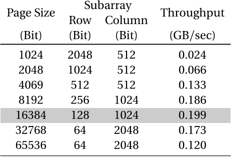
  • In detail, Table 4.1 shows the row and column address bits matched to each page size.
  • While the page size change, the authors also change subarray size in each wordline and bitline direction from 25 bit to 212 bit.
  • The geometry change caused wordline and bitline length to change along with the shift in driving peripheral circuit size.

4.2 3D Design Space Exploration in 35 nm Node

  • A DRAM rank is a group of DRAM devices which respond and operate at the same time by the single command.
  • Figure 4.8a shows a traditional planar DRAM, which, in this case, the rank is a single die.
  • Compared to the TSV area in Figure 4.9, this makes single bank splitting more expensive than the fine-grained rank-level stacking in terms of area and power.
  • The logic die could be designed and fabricated by using another process to achieve best operation performance.
  • This is beyond DATE model’s evaluation range.

4.2.1 Area Efficiency

  • As discussed in Section 4.1.1.1, as space for the peripheral circuit and additional functions is increased, area efficiency is decreased.
  • As the number of layers increases, the memory size to be allocated per die to maintain 1 Gb becomes smaller (i.e., the cell array size per die is reduced).
  • The number of data and control signals is similar even if the number of 1The figure is used under author’s permission.
  • Thus the number of TSVs for data and control signals is similar even as the number of die increases.
  • Since the TSV area for data and control signal is almost the same, and the area of the cell area is reduced, the area efficiency deteriorates as the number of dies increases in both 6 F 2 and 4 F 2 layout case.

4.2.2 Energy Efficiency

  • Table 4.19 shows the best energy efficiency on each 3D stacked DRAM configuration as the number of layers is increased.
  • In the other cases, the best energy efficiency design had 2.
  • Mb bank size which was the smallest bank size examined during the evaluation.
  • In all cases, wire energy and TSV energy accounted for approximately 88 to 95 percent of the entire read energy consumption, which indicates that the logic energy was optimized.
  • As the number of stacked die increased, the TSV energy started to dominate overall wire energy since the TSV energy increased proportional to the number of layers.

4.2.3 Throughput

  • Table 4.20 shows the best throughput on each 3D stacked DRAM as the number of stacked die is increased.
  • After the eight-layer, the DRAM throughput exhibited diminishing returns.
  • As discussed in Section 4.1.2.3, the smaller the bank size, faster throughput was observed.
  • I/O and miscellaneous indicates I/O transceiver and control signal delay.
  • Decoder indicates the sum of row and column address decoder delay.

4.2.4 Product of Design Metric

  • Figure 4.13 shows the tendency of the best result of the combinations of area efficiency (AE), energy efficiency (EE), and throughput (TH) as the die count is varied.
  • This tendency of the area efficiency also affects the combined design metric.
  • Compared to planar design and four layered DRAM design, the area efficiency decreased approximately 48% while energy efficiency increased approximately 50%.
  • The VCAT-base design displayed better throughput than the RCAT-base design in all cases, and the RCAT-based design displayed better area efficiency than the VCAT-based design in all cases.
  • Thus, the RCAT-based design 114 115 exhibited better performances after that point.

4.2.5 Design Metric Comparison in Different Technology

  • Figure 4.14 shows the design metric peak value comparison between 16 nm, 35 nm, and 68 nm node when the die count is increased.
  • Figure 4.14c presents the best throughput for various process node as the die count is increased.
  • In the case of area efficiency, 4 F 2 cell layout DRAM design exhibited the smaller area with 68.0% area efficiency compared the 6 F 2 layout.
  • For the throughput, the RCAT-based design exhibited the optimum point when the die count was eight while VCAT-based design also exhibited the optimum with eight dies.

5.1 Summary of Contributions

  • The authors have presented the three dimensional DRAM Area, Timing, and Energy model.
  • The authors have proposed a wire roadmap using the material parameters provided through ITRS roadmap [20] and the physical dimensions presented in the ITRS roadmap and the cross-sectional die report [51].
  • The metal layer 2 and 3 are predicted larger size, therefore resistance values of DATE roadmap are smaller than the logic processes and capacitance values of DATE roadmap are more significant than the logic process.
  • The authors have implemented and verified circuit level modeling: The logic and buffer size was determined using the logical effort [54].

Did you find this useful? Give us your feedback

Content maybe subject to copyright    Report

ABSTRACT
PARK, JONG BEOM. 3D-DATE: A Circuit-Level Three-Dimensional DRAM Area, Timing,
and Energy Model. (Under the direction of W. Rhett Davis and Paul D. Franzon.)
Three-dimensional stacked DRAM technology has emerged recently. Many studies have
shown that 3D DRAM is most promising solutions for future memory architecture to fulfill
high bandwidth and high-speed operation with low energy consumption. It is necessary
to explore 3D DRAM design space and find the optimum DRAM architecture in different
system needs. However, a few studies have offered models for power and access latency
calculations of DRAM designs in limited ranges. This has led to a growing gap in knowledge
of the area, timing, and energy modeling of 3D DRAMs for utilization in the design process
of processor architectures that could benefit from 3D DRAMs. This paper presents a circuit
level DRAM Area, Timing, and Energy model (DATE) which supports 3D DRAM design with
TSV. DATE provides front-end and back-end DRAM process roadmap from 90 nm to 16 nm
node and provides a broader range 3D DRAM design model along with emerging transistor
device. DATE is successfully validated against several commodity planar and 3D DRAMs
and published prototype DRAMs with emerging device. Energy verification has a mean
error of about -5% to 1%, with a standard deviation of up to 9.8%. Speed verification has
a mean error of about -13% to -27% and a standard deviation of up to 24%. In the case of
the area, the bank has a mean error of -3% and the whole die has a mean error of -1%. The
standard deviation for area is up to 4.2%. In the case study, we demonstrate that 1Gb DDR3
DRAM designs achieve up to about 0.7 Gb/sec data throughput and energy efficiency of
510 bit/nJ using 3D design options with 16 nm DRAM technology.

© Copyright 2018 by Jong Beom Park
All Rights Reserved

3D-DATE: A Circuit-Level Three-Dimensional DRAM Area, Timing, and Energy Model
by
Jong Beom Park
A dissertation submitted to the Graduate Faculty of
North Carolina State University
in partial fulfillment of the
requirements for the Degree of
Doctor of Philosophy
Electrical Engineering
Raleigh, North Carolina
2018
APPROVED BY:
James Tuck Hans Hallen
W. Rhett Davis
Co-chair of Advisory Committee
Paul D. Franzon
Co-chair of Advisory Committee

DEDICATION
My Lord, Jesus
My wife, Jina, and my family.
ii

BIOGRAPHY
Jong Beom Park was born in Seoul, Korea in March 1978. He earned a Bachelors of Science
at Hanyang University at Ansan in 2001. In 2003, he earned a Master of Science in Electronic,
Electrical, Control and Instrumentation Engineering from Hanyang University at Seoul in
2003, with a thesis entitled "Implementation of the Multirate Viterbi Algorithm for IEEE
802.11a Wireless LAN System." After working in the industry for several years, Mr. Park
entered the ECE graduate program at North Carolina State University in 2009, where he
earned a Masters of Science in Computer Engineering from North Carolina State University
in 2010. He initiated his Ph.D. studies in Electrical Engineering in 2011 working on the
NSF’s Underwater Optical Communication program with Dr. John Muth. In 2012, Mr. Park
switched his research focus to the circuit design area rather than embedded system. Thus,
he joined Dr. Paul D. Franzons research group in 2012. He started working on the DARPA
PERFECT program in 2012 and 2013, focusing on the design of a custom, low power memory.
Mr. Park also maintains an active interest in computer architecture, digital VLSI design,
and machine learning.
iii

Citations
More filters
Proceedings ArticleDOI
14 Jun 2021
TL;DR: Sieve as mentioned in this paper proposes three DRAM-based in-situ k-mer matching accelerator designs (one optimized for area, one optimized for throughput, and one that strikes a balance between hardware cost and performance), which leverage a novel data mapping scheme to allow for simultaneous comparisons of millions of DNA base pairs.
Abstract: The rapid influx of biosequence data, coupled with the stagnation of the processing power of modern computing systems, highlights the critical need for exploring high-performance accelerators that can meet the ever-increasing throughput demands of modern bioinformatics applications. This work argues that processing in memory (PIM) is an effective solution to enhance the performance of k-mer matching, a critical bottleneck stage in standard bioinformatics pipelines, that is characterized by random access patterns and low computational intensity. This work proposes three DRAM-based in-situ k-mer matching accelerator designs (one optimized for area, one optimized for throughput, and one that strikes a balance between hardware cost and performance), dubbed Sieve, that leverage a novel data mapping scheme to allow for simultaneous comparisons of millions of DNA base pairs, lightweight matching circuitry for fast pattern matching, and an early termination mechanism that prunes unnecessary DRAM row activation to reduce latency and save energy. Evaluation of Sieve using state-of-the-art workloads with real-world datasets shows that the most aggressive design provides an average of 326x/32x speedup and 74X/48x energy savings over multi-core-CPU/GPU baselines for k-mer matching.

15 citations

Journal ArticleDOI
TL;DR: The molybdenum tungsten/amorphous InGaZnO (a-IGZO)/TiO2/n-type Si-based resistive random access memory (ReRAM) manufactured reduced conductivity and prevented an increase in leakage current caused by oxygen vacancies with sufficient recovery of the metal-oxygen bond.
Abstract: In this study, molybdenum tungsten/amorphous InGaZnO (a-IGZO)/TiO2/n-type Si-based resistive random access memory (ReRAM) is manufactured. After deposition of the a-IGZO, annealing was performed at 200, 300, 400, and 500 °C for approximately 1 h in order to analyze the effect of temperature change on the ReRAM after post annealing in a furnace. As a result of measuring the current-voltage curve, the a-IGZO/TiO2-based ReRAM annealed at 400 °C reached compliance current in a low-resistance state, and showed the most complete hysteresis curve. In the a-IGZO layer annealed at 400 °C, the O1/Ototal value increased most significantly, to approximately 78.2%, and the O3/Ototal value decreased the most, to approximately 2.6%. As a result, the a-IGZO/TiO2-based ReRAM annealed at 400 °C reduced conductivity and prevented an increase in leakage current caused by oxygen vacancies with sufficient recovery of the metal-oxygen bond. Scanning electron microscopy analysis revealed that the a-IGZO surface showed hillocks at a high post annealing temperature of 500 °C, which greatly increased the surface roughness and caused the surface area performance to deteriorate. Finally, as a result of measuring the capacitance-voltage curve in the a-IGZO/TiO2-based ReRAM in the range of -2 V to 4 V, the accumulation capacitance value of the ReRAM annealed at 400 °C increased most in a nonvolatile behavior.

13 citations

Book ChapterDOI
Ravi Mahajan1, Bob Sankman1
01 Jan 2017
TL;DR: The advantages and limitations of 3D architectures are discussed to provide context for why 3D stacking has become a key area of interest for product architects, why it has generated broad industry attention, and why its adoption has been tenous.
Abstract: In this chapter, the advantages and limitations of 3D architectures are discussed to provide context for why 3D stacking has become a key area of interest for product architects, why it has generated broad industry attention, and why its adoption has been tenous. The primary focus of this chapter is on 3D architectures that use Through Silicon Vias (TSVs), while other System In Package (SIP) architectures that do not rely on TSVs are discussed for completeness. The key elements of a TSV-based 3D architecture are described, followed by a description of the three methods of manufacturing wafers with TSVs (i.e., Via-First, Via-Middle, and Via-Last). An analysis of the different assembly process flows for 3D structures, broadly classified as (a) Wafer-to-Wafer (W2W), (b) Die-to-Wafer (D2W), and (c) Die-to-Die (D2D) assembly processes, is covered. Key design, assembly process, test process, and materials considerations for each of these flows are described. The chapter concludes with a discussion of current and anticipated challenges for 3D architectures.

11 citations

Proceedings ArticleDOI
28 May 2022
TL;DR: In this article , the authors proposed a 12-bit high dynamic range floating-point format called TinyFloat that reduces the total number of data access energy by 20% compared to IEEE 754 half and single precision.
Abstract: Deep Neural Network (DNN) training consumes high-energy. On the other hand, DNNs deployed on edge devices demand very high-energy efficiency. In this context, Processing-in-Memory (PIM) is an emerging compute paradigm that bridges the memory-computation gap to improve the energy-efficiency. DRAMs are one such memory type employed for designing energy-efficient PIM architectures for DNN training. One of the major issues of DRAM-PIM architectures designed for DNN training is the high number of internal data accesses within a bank between the memory arrays and the PIM computation units (e.g. 51% more than inference). These internal data accesses in the state-of-the-art DRAM PIM architectures consume very high energy compared to computation units. Hence, it is important to reduce the internal data access energy within the DRAM bank for further improving the energy efficiency of DRAMPIM architectures. We present three novel optimizations that together reduce the internal data access energy up to 81.54%. Our first optimization modifies the bank data access circuit to enable partial accesses of data instead of the conventional fixed granularity accesses, thereby exploiting the available sparsity during training. The second optimization is to have a dedicated low-energy region within the DRAM bank that has low capacitive load of global wires and shorter data movement. Finally, we propose a 12-bit high dynamic range floating-point format called TinyFloat that reduces the total number of data access energy by 20% compared to IEEE 754 half and single precision.

2 citations

References
More filters
Book
01 Jan 1996
TL;DR: In this paper, the authors present a survey of the state-of-the-art in the field of digital integrated circuits, focusing on the following: 1. A Historical Perspective. 2. A CIRCUIT PERSPECTIVE.
Abstract: (NOTE: Each chapter begins with an Introduction and concludes with a Summary, To Probe Further, and Exercises and Design Problems.) I. THE FABRICS. 1. Introduction. A Historical Perspective. Issues in Digital Integrated Circuit Design. Quality Metrics of a Digital Design. 2. The Manufacturing Process. The CMOS Manufacturing Process. Design Rules-The Contract between Designer and Process Engineer. Packaging Integrated Circuits. Perspective-Trends in Process Technology. 3. The Devices. The Diode. The MOS(FET) Transistor. A Word on Process Variations. Perspective: Technology Scaling. 4. The Wire. A First Glance. Interconnect Parameters-Capitance, Resistance, and Inductance. Electrical Wire Models. SPICE Wire Models. Perspective: A Look into the Future. II. A CIRCUIT PERSPECTIVE. 5. The CMOS Inverter. The Static CMOS Inverter-An Intuitive Perspective. Evaluating the Robustness of the CMOS Inverter: The Static Behavior. Performance of CMOS Inverter: The Dynamic Behavior. Power, Energy, and Energy-Delay. Perspective: Technology Scaling and Its Impact on the Inverter Metrics. 6. Designing Combinational Logic Gates in CMOS. Static CMOS Design. Dynamic CMOS Design. How to Choose a Logic Style? Perspective: Gate Design in the Ultra Deep-Submicron Era. 7. Designing Sequential Logic Circuits. Timing Metrics for Sequential Circuits. Classification of Memory Elements. Static Latches and Registers. Dynamic Latches and Registers. Pulse Registers. Sense-Amplifier Based Registers. Pipelining: An Approach to Optimize Sequential Circuits. Non-Bistable Sequential Circuits. Perspective: Choosing a Clocking Strategy. III. A SYSTEM PERSPECTIVE. 8. Implementation Strategies for Digital ICS. From Custom to Semicustom and Structured-Array Design Approaches. Custom Circuit Design. Cell-Based Design Methodology. Array-Based Implementation Approaches. Perspective-The Implementation Platform of the Future. 9. Coping with Interconnect. Capacitive Parasitics. Resistive Parasitics. Inductive Parasitics. Advanced Interconnect Techniques. Perspective: Networks-on-a-Chip. 10. Timing Issues in Digital Circuits. Timing Classification of Digital Systems. Synchronous Design-An In-Depth Perspective. Self-Timed Circuit Design. Synchronizers and Arbiters. Clock Synthesis and Synchronization Using a Phased-Locked Loop. Future Directions and Perspectives. 11. Designing Arithmetic Building Blocks. Datapaths in Digital Processor Architectures. The Adder. The Multiplier. The Shifter. Other Arithmetic Operators. Power and Spped Trade-Offs in Datapath Structures. Perspective: Design as a Trade-off. 12. Designing Memory and Array Structures. The Memory Core. Memory Peripheral Circuitry. Memory Reliability and Yield. Power Dissipation in Memories. Case Studies in Memory Design. Perspective: Semiconductor Memory Trends and Evolutions. Problem Solutions. Index.

2,744 citations


"3-D-DATE: A Circuit-Level Three-Dim..." refers methods in this paper

  • ...1) Repeater Model: Rabaey’s approach [45] is adopted for the repeater model in 3D-DATE....

    [...]

  • ...For the energy calculation of the gate, 3D-DATE accounts for the consumed charge by adding the capacitance of every node since the dissipated energy is given by the equation [45]:...

    [...]

Journal ArticleDOI
TL;DR: It is found possible to define delay time and rise time in such a way that these quantities can be computed very simply from the Laplace system function of the network.
Abstract: When the transient response of a linear network to an applied unit step function consists of a monotonic rise to a final constant value, it is found possible to define delay time and rise time in such a way that these quantities can be computed very simply from the Laplace system function of the network. The usefulness of the new definitions is illustrated by applications to low pass, multi‐stage wideband amplifiers for which a number of general theorems are proved. In addition, an investigation of a certain class of two‐terminal interstage networks is made in an endeavor to find the network giving the highest possible gain—rise time quotient consistent with a monotonic transient response to a step function.

1,693 citations


"3-D-DATE: A Circuit-Level Three-Dim..." refers methods in this paper

  • ...By using Elmore delay approach [61], propagation delay of the interconnect is given as: tp ,c r i t =m (0....

    [...]

Journal ArticleDOI
01 Apr 2001
TL;DR: Wires that shorten in length as technologies scale have delays that either track gate delays or grow slowly relative to gate delays, which is good news since these "local" wires dominate chip wiring.
Abstract: Concern about the performance of wires wires in scaled technologies has led to research exploring other communication methods. This paper examines wire and gate delays as technologies migrate from 0.18-/spl mu/m to 0.035-/spl mu/m feature sizes to better understand the magnitude of the the wiring problem. Wires that shorten in length as technologies scale have delays that either track gate delays or grow slowly relative to gate delays. This result is good news since these "local" wires dominate chip wiring. Despite this scaling of local wire performance, computer-aided design (CAD) tools must still become move sophisticated in dealing with these wires. Under scaling, the total number of wires grows exponentially, so CAD tools will need to handle an ever-growing percentage of all the wires in order to keep designer workloads constant. Global wires present a more serious problem to designers. These are wires that do not scale in length since they communicate signals across the chip. The delay of these wives will remain constant if repeaters are used meaning that relative to gate delays, their delays scale upwards. These increased delays for global communication will drive architectures toward modular designs with explicit global latency mechanisms.

1,486 citations


"3-D-DATE: A Circuit-Level Three-Dim..." refers methods in this paper

  • ...3D-DATE adopts Horowitz wire model [43] for calculating resistance and capacitance of wire....

    [...]

01 Jan 2009
TL;DR: This report details the analytical model assumed for the newly added modules along with their validation analysis of CACTI 6.0, a significantly enhanced version of the tool that primarily focuses on interconnect design for large caches.
Abstract: © CACTI 6.0: A Tool to Model Large Caches Naveen Muralimanohar, Rajeev Balasubramonian, Norman P. Jouppi HP Laboratories HPL-2009-85 No keywords available. Future processors will likely have large on-chip caches with a possibility of dedicating an entire die for on-chip storage in a 3D stacked design. With the ever growing disparity between transistor and wire delay, the properties of such large caches will primarily depend on the characteristics of the interconnection networks that connect various sub-modules of a cache. CACTI 6.0 is a significantly enhanced version of the tool that primarily focuses on interconnect design for large caches. In addition to strengthening the existing analytical model of the tool for dominant cache components, CACTI 6.0 includes two major extensions over earlier versions: first, the ability to model Non-Uniform Cache Access (NUCA), and second, the ability to model different types of wires, such as RC based wires with different power, delay, and area characteristics and differential low-swing buses. This report details the analytical model assumed for the newly added modules along with their validation analysis. External Posting Date: April 21, 2009 [Fulltext] Approved for External Publication Internal Posting Date: April 21, 2009 [Fulltext] Published in International Symposium on Microarchitecture, Chicago, Dec 2007. Copyright International Symposium on Microarchitecture, 2007. CACTI 6.0: A Tool to Model Large Caches Naveen Muralimanohar, Rajeev Balasubramonian, Norman P. Jouppi † School of Computing, University of Utah ‡ Hewlett-Packard Laboratories Abstract Future processors will likely have large on-chip caches with a possibility of dedicating an entire die for on-chip storage in a 3D stacked design. With the ever growing disparity between transistor and wire delay, the properties of such large caches will primarily depend on the characteristics of the interconnection networks that connect various sub-modules of a cache. CACTI 6.0 is a significantly enhanced version of the tool that primarily focuses on interconnect design for large caches. In addition to strengthening the existing analytical model of the tool for dominant cache components, CACTI 6.0 includes two major extensions over earlier versions: first, the ability to model Non-Uniform Cache Access (NUCA), and second, the ability to model different types of wires, such as RC based wires with different power, delay, and area characteristics and differential low-swing buses. This report details the analytical model assumed for the newly added modules along with their validation analysis.Future processors will likely have large on-chip caches with a possibility of dedicating an entire die for on-chip storage in a 3D stacked design. With the ever growing disparity between transistor and wire delay, the properties of such large caches will primarily depend on the characteristics of the interconnection networks that connect various sub-modules of a cache. CACTI 6.0 is a significantly enhanced version of the tool that primarily focuses on interconnect design for large caches. In addition to strengthening the existing analytical model of the tool for dominant cache components, CACTI 6.0 includes two major extensions over earlier versions: first, the ability to model Non-Uniform Cache Access (NUCA), and second, the ability to model different types of wires, such as RC based wires with different power, delay, and area characteristics and differential low-swing buses. This report details the analytical model assumed for the newly added modules along with their validation analysis.

845 citations


"3-D-DATE: A Circuit-Level Three-Dim..." refers background in this paper

  • ...1 [46] and described in Rambus model [10]....

    [...]

  • ...1 and Horowitz to analyze delay of bitline, sense amplifier, and write-back driver [46], [48]....

    [...]

  • ...Nine bit row address decoding path [10], [46]....

    [...]

Journal ArticleDOI
TL;DR: In this paper, an analytical model for the access and cycle times of on-chip direct-mapped and set-associative caches is presented, where the inputs to the model are the cache size, block size, and associativity, as well as array organization and process parameters.
Abstract: This paper describes an analytical model for the access and cycle times of on-chip direct-mapped and set-associative caches. The inputs to the model are the cache size, block size, and associativity, as well as array organization and process parameters. The model gives estimates that are within 6% of Hspice results for the circuits we have chosen. This model extends previous models and fixes many of their major shortcomings. New features include models for the tag array, comparator, and multiplexor drivers, nonstep stage input slopes, rectangular stacking of memory subarrays, a transistor-level decoder model, column-multiplexed bitlines controlled by an additional array organizational parameter, load-dependent size transistors for wordline drivers, and output of cycle times as well as access times. Software implementing the model is available via ftp.

829 citations

Frequently Asked Questions (2)
Q1. What are the contributions in this paper?

This paper presents a circuit level DRAM Area, Timing, and Energy model ( DATE ) which supports 3D DRAM design with TSV. In the case study, the authors demonstrate that 1Gb DDR3 DRAM designs achieve up to about 0. 7 Gb/sec data throughput and energy efficiency of 510 bit/nJ using 3D design options with 16 nm DRAM technology. 

There are several interesting directions in future research. It would also be interesting to extend DATE model for evaluating the finegrained 3D DRAM design by adding high-performance transistor roadmap. “ The future of wires ”. For the device roadmap, the authors believe it would be interesting to update current roadmap with emerging devices such as FinFET-based gate transistors or emerging materials for the wire, which would impact overall speed.