All figures (21)
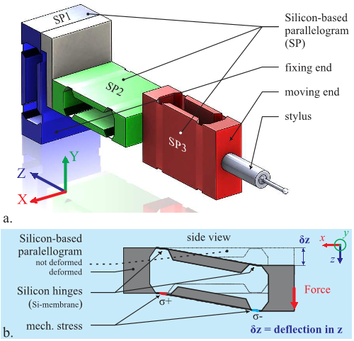 Fig. 1. a. Schematic of the 3DSP microprobe with stylus, and b. illustration of a SP deflected in its soft axis (z) direction.1
 Fig. 5. a.-c. Deflection of a 3DSP in -, -, and -direction and d. deflection of a SP in -direction as obtained by simulations for a force of 50 mN.
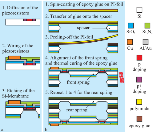 Fig. 6. a. Wafer-level fabrication of piezoresistors and silicon membranes and b. wafer-level adhesive bonding process with glue transfer for the fabrication of parallelograms.
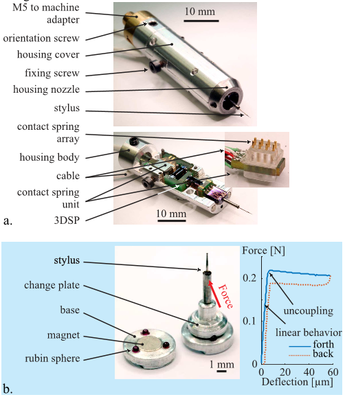 Fig. 13. a. Housing for a 3DSP, and b. stylus changing system and it mechanical behavior
 Fig. 7. a. First prototype of the 3DSP with and without PIfoil for wiring, b. detail view showing the foil peel-off from the glass wafer after processing and laser cutting, c. assembly of SP and PI-foil with soldering tool, and d. adhesive assembly of SP3 with SP2 using a vacuum assisted tool.
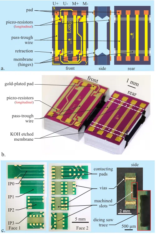
 Fig. 11. Detail views of the components of the microprobe assembled with interposers: a. front, rear and side view of the new SP design with pass-through tracks, b. photograph of new SPs, and c. face 1, face 2 and side view of the interposers made of FR4
 Fig. 12. Illustration of the one-step assembly and soldering of the new 3DSP: a. schematic of the vacuum assisted tool without and with assembled SPs and IPs, b. photograph showing assembly of the 3DSP using the tool, and c. photograph showing soldering the SPs on the IPs.
 Fig. 2. a. Schematic of the top and side view of the SP with four wired piezoresistors. The geometric parameters varied in simulations are given in framed boxes. b. Schematic of the Wheatstone bridge with piezoresistors (R1, R2, R3, R4) and the corresponding nodes for the excitation voltage (U+, U-) and the output signal (M+, M-). c. Photograph of SP with longitudinal piezoresistors connected to a PCB for characterization.
 Fig. 16. Comparison of achieved measuring ranges and anisotropies for the new 3DSP with some microprobes described in the literature.
 Table 4. Measured stiffness in -, -, and -direction for a 3DSP w/ and w/o stylus.
 Table 5. Measured sensitivities in -, -, and -direction for a 3DSP w/ and w/o stylus.
 Fig. 8. a. Force versus deflection measurement for a single
 Fig. 9. Simulated and measured stiffness values together with the corresponding deflection in -direction leading to fracture for single SPs with a membrane thickness of 19.1 µm.
 Fig. 3. a. Deformation of the SP and definition of the three segments I, II and III, b. mechanically equivalent beam segment model and, c. FEM simulated, analytically obtained and measured deflections ( ) of an SP when a force of 2P= 50 mN is applied at the free end.
 Fig. 14. a. Voltage/deflection diagram of a single SP for a ±200 µm deflection range (insert showing the measurement setup with two obstacles and optical determination of SP deflection), and b. zoom in around the point of deflection reversal (±2 µm) reveals a dead zone with a more scattered signal.
 Table 3. Mechanical and sensory characterization of three SP from a single lot.
 Fig. 15. Force/deflection diagram of a 3DSP for a 100 µm deflection range in -, -, and -direction: a. without, b.
 Table 2. Measured stiffnesses S and sensitivities E in X-, Y- and Z-direction for the 3DSP prototypes w/ and w/o foil.
 Fig. 10. a. Photograph of the new 3D silicon based parallelogram microprobe with a 300µm stylus tip, b. assembly and wiring of the three SPs with interposers (IPs), and b. diagram illustrating the electrical signal circuit.
 Table 1. Fit parameters, as obtained by simulations for studying sensitivities of the hinge dimensions. The results are given for the stiffnesses in N·mm-1 and for the parameters given in mm.
 Fig. 4. Single Si-parallelogram stiffness a. in , (hard) directions and b. in (soft) direction as a function of 5CDC and BCDC for ECDC = 3.8 , as obtained by simulations. The hard axis stiffnesses FI , 67> FJ typically differ by an order of magnitude and are therefore plotted on different scales.