scispace - formally typeset
Search or ask a question
Journal ArticleDOI

α-alumina coatings on WC/Co substrates by physical vapor deposition

TL;DR: Physical vapor deposition coatings for cutting tools may be deposited by, e.g., reactive magnetron sputtering, which gives rise to problems due to insulating layers on surfaces.
Abstract: Physical vapor deposition coatings for cutting tools may be deposited by, e.g. reactive magnetron sputtering. Alumina growth in Ar/O2 gas mixtures gives rise to problems due to insulating layers on ...

Summary (1 min read)

Introduction

  • Hard physical vapor deposited (PVD) coatings may be coated by a variety of methods, e.g. direct current (DC) magnetron sputtering in Ar inert gas.
  • Albeit stable, BPDMS has only been repeatedly successful in depositing γ-alumina, which is a drawback if phase stability of the coating is of concern.
  • So far, commercial α-alumina coatings have only been grown by chemical vapor deposition (CVD) at relatively high substrate temperatures.
  • Therefore one drawback with HiPIMS has been the inherently low growth rate.
  • Recently, it was shown that high rate sputtering is possible, and that long time stable operation of Ar/O2 discharges is possible without feedback control of the reactive gas [12].

Experimental details

  • Coatings were made in a laboratory scale ultra-high vacuum system, with a base pressure of less than 3×10⁻⁵ Pa.
  • Cemented carbide, WC10%Co (H10F), substrates were mounted flat on a resistive heater directly above the magnetron, at a distance of 11 cm.
  • The temperature reported herein is always the set nominal temperature, however, not the estimated temperature.
  • To the extent of the analyses performed in the present work the process was reproducible, in that consecutive runs under the Page 4 of 18 same conditions yielded coatings with similar properties.
  • TEM cross-section samples were produced by means of classical sample preparation by first mechanical dimpling with diamond particles and finally thinned to electron transparency by Ar ion etching.

On the HiPIMS Process

  • HiPIMS resembles ordinary magnetron sputtering in many aspects.
  • In many cases the sputtering yield is lower for the compound now covering the target, and the deposition rate drops.
  • These coatings were deposited at 650ºC nominal temperature, but it is estimated that the real extending almost throughout the total film thickness.
  • XRD of this particular sample did, however, not indicate anything else but a pure α-alumina coating, a fact probably due to a very small γ-grain size.
  • Since it is anticipated that alumina will improve the chemical stability of the tool surface on which the chips flow a test was selected that emphasizes the wear on the rake face.

Conclusions

  • In this study the HiPIMS technique was used to deposit alumina coatings on WC/Co substrates and tools.
  • Α-alumina was succesfully deposited on WC/Co substrates at 650 °C. .
  • The deposition rate was found to be independent of substrate bias and substrate temperature in the range of 500 to 650 °C. .
  • The crystalline structure depended on deposition temperature.
  • Hence, these first tests are promising in terms of the potential for using HiPIMS deposited alumina as a wear-resistant coating in metal cutting applications.

Did you find this useful? Give us your feedback

Content maybe subject to copyright    Report



Linköping University Post Print


α-alumina coatings on WC/Co substrates by
physical vapor deposition


T.I. Selinder, E. Coronel, Erik Wallin and Ulf Helmersson




N.B.: When citing this work, cite the original article.



Original Publication:
T.I. Selinder, E. Coronel, Erik Wallin and Ulf Helmersson, α-alumina coatings on WC/Co
substrates by physical vapor deposition, 2009, International journal of refractory metals
& hard materials, (27), 2, 507-512.
http://dx.doi.org/10.1016/j.ijrmhm.2008.10.007
Copyright: Elsevier Science B.V., Amsterdam.
http://www.elsevier.com/
Postprint available at: Linköping University Electronic Press
http://urn.kb.se/resolve?urn=urn:nbn:se:liu:diva-15359

α-ALUMINA COATINGS ON WC/Co SUBSTRATES BY PHYSICAL VAPOR
DEPOSITION
T.I. Selinder*, E. Coronel*, E. Wallin**, U. Helmersson**
*Sandvik Tooling, SE-126 80 Stockholm, Sweden
**Plasma and Coatings Physics Division, IFM Material Physics, Linköping University,
SE-581 83 Linköping, Sweden
Abstract
Physical vapor deposition coatings for cutting tools may be deposited by, e.g. reactive
magnetron sputtering. Alumina growth in Ar/O
2
gas mixtures gives rise to problems due
to insulating layers on targets, and hysteresis effects with respect to oxygen gas flow. In
this paper is described a technology for the deposition of crystalline alumina: reactive
high power impulse magnetron sputtering. Pure Al was used as target material, and the
cemented carbide (WC/Co) substrates were kept at 500-650ºC. Hysteresis effects with
respect to oxygen gas flow were alleviated, which enabled stable growth at a high
deposition rate. The high power impulses were helpful in obtaining a crystalline oxide
coating. X-ray diffraction and cross-section transmission electron microscopy showed
that α-alumina films were formed. Technological testing of these PVD alumina
coatings, with state-of-the-art AlTiN as benchmark, showed significantly improved
crater wear resistance in steel turning.
Keywords: HiPIMS, HPPMS, ionized-PVD, alumina, corundum
Page 1 of 18

Introduction
Hard physical vapor deposited (PVD) coatings may be coated by a variety of methods,
e.g. direct current (DC) magnetron sputtering in Ar inert gas. Reactive sputtering in
Ar/oxygen gas mixtures, may be used to grow oxides, but for insulators, in particular
alumina, this gives rise to problems due to the formation of insulating layers.
Conducting surfaces are a prerequisite to sustain an electrical glow discharge in DC
mode. These problems are circumvented in the bipolar pulsed magnetron technique
(BPDMS) [1-2], in which two magnetrons work in pair, alternating as anode and
sputtering target. By using pulse frequencies in the range of a few kHz the Al erosion
rate exceeds the rate of oxide formation at each target surface. Albeit stable, BPDMS
has only been repeatedly successful in depositing γ-alumina, which is a drawback if
phase stability of the coating is of concern. So far, commercial α-alumina coatings have
only been grown by chemical vapor deposition (CVD) at relatively high substrate
temperatures. In order to coat heat sensitive substrates, e.g. polycrystalline c-BN, high
speed steel, brazed tools, etc. the process temperature needs to be reduced. For this and
other reasons research and development on PVD alumina by, for instance, dual
magnetron sputtering [3], and arc evaporation [4] has been intense for the past few
years. Preoxidation of Cr-containing surfaces have enabled nucleation and growth of α-
alumina [5], but still requires substrate temperatures of 700-750ºC. A commercial
technology capable of growing highly crystalline mixed oxides (Al,Cr)
2
O
3
by the arc
method at temperatures below 600ºC were recently made available on the market [6],
but the commercialization of pure PVD α-alumina still remains. In this context the
novel technology high power impulse magnetron sputtering (HiPIMS) [7,8]have been
studied because this intermittent very high energetic sputtering technique widens the
Page 2 of 18

possibilities of supplying energy to the growth surface, which likely is the key to
success in nucleating α-alumina, and sustaining its growth. The HiPIMS technique has
been studied for deposition of both conducting coatings [9] as well as for oxide coatings
[10-11]. The degree of ionization of the sputtered material may be higher than for
traditional sputtering but the ionized species also accelerate towards the target, so-called
self sputtering, that has a lower sputtering yield than that of Ar sputtering. Therefore
one drawback with HiPIMS has been the inherently low growth rate. Recently, it was
shown that high rate sputtering is possible, and that long time stable operation of Ar/O
2
discharges is possible without feedback control of the reactive gas [12]. Stoichiometric
alumina was grown, with a phase structure that was dependent on substrate temperature;
at temperatures as low as 650ºC α-alumina was the only crystalline phase detected by
X-ray diffraction (XRD). Initial transmission electron microscopy (TEM) studies
revealed, however, that γ-alumina may grow, at least during the early stages in film
growth directly on WC/Co. XRD indicates that at the same temperature and identical
growth conditions AlTiN pre-coated substrates tend to favor growth of α- over γ-
alumina. A possible origin of this difference is discussed.
Experimental details
Coatings were made in a laboratory scale ultra-high vacuum system, with a base
pressure of less than 3×10
-5
Pa. A planar, 50mm diameter shuttered magnetron
sputtering source was mounted with a pure (99.999%) 3mm thick Al target. Cemented
carbide, WC10%Co (H10F), substrates were mounted flat on a resistive heater directly
above the magnetron, at a distance of 11 cm. Temperatures during different runs were
maintained at 650, 575, and 500 ºC. In order to grow films on cutting edges ISO style
Page 3 of 18

CNMG120408-MM H10F substrates were mounted, two at a time, on a tilted holder.
One nose and cutting edge was directed towards the magnetron. In this way both the
tool rake and flank faces were coated. In the latter case, however, it is estimated that the
real substrate temperature is approx. 50ºC less than the nominal set value. The
temperature reported herein is always the set nominal temperature, however, not the
estimated temperature. Substrates were either floating, or bias was applied by radio
frequency (RF) by an Advanced Energy RFX-600 power supply.
A fixed 99.997% pure Ar flow was adjusted to establish a pressure of 2.7 Pa. The
substrates were sputter etched for 15 minutes in an RF glow discharge resulting in a
-175 V DC bias of the sample holder, after which the pressure was reduced to 0.8 Pa,
and the sputtering initiated with the shutter closed. Sputtering was carried out by means
of a DC voltage source pulsed by a Melec SPIK1000A unit. The Al target was sputtered
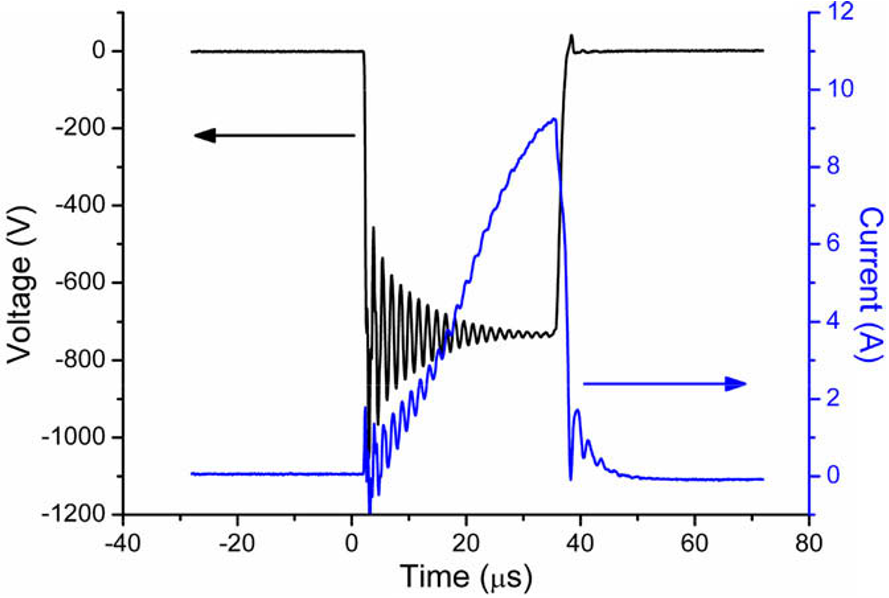
at an average power of 110W (~5 Wcm
-2
) in pulses having a peak power in excess of
6kW, or 300 Wcm
-2
. The process working point was controlled by selecting the
99.9995% pure oxygen flow, to a value of approximately 2% of the Ar flow. The
oxygen flow was determined empirically so that transparent coatings were deposited. It
is expected that substrate oxidation during this stage is low: As the oxygen was
introduced when the discharge was running with the shutter closed it is reasonably
assumed that the partial pressure of oxygen is low in the deposition chamber; in the
working point chosen it is to a large extent consumed, incorporated in the growing film.
Also, there were no visible discolorations, after coating runs, of uncoated substrate
surfaces exposed to the sputtering atmosphere. To the extent of the analyses performed
in the present work the process was reproducible, in that consecutive runs under the
Page 4 of 18
Citations
More filters
Journal ArticleDOI
TL;DR: In this article, a corundum-structured metastable solid solution alpha-(Cr,Al)(2)O-3 with Cr/Al ratios of 2-10 was grown with a dense, fine-grained morphology.

63 citations

Journal ArticleDOI
TL;DR: In this paper, a combinatorial experimental approach was chosen to describe the growth and microstructure evolution of Al-Cr-O thin films by means of reactive r.f. magnetron sputtering.
Abstract: The development of new coatings with superior functionalities for high performance cutting tools is a key challenge in manufacturing. In this context, the synthesis of aluminium oxide and derivative oxide thin films is attracting large scientific and technical interests. The present paper addresses fundamental materials science-based aspects of the physical vapour deposition (PVD) growth of Al–Cr–O thin films at a substrate temperature of 500 °C. A combinatorial experimental approach was chosen to describe the growth and microstructure evolution of Al–Cr–O thin films by means of reactive r.f. magnetron sputtering. A segmented target consisting of two half plates of Al and Cr was used for the deposition carried out under stationary conditions in a laboratory-scale PVD coater. Opposite to the cathode five substrate samples were placed in a line. The r.f. cathode power was set to 500 W and the r.f. substrate bias was set to − 100 V. The total gas pressure was kept constant at 0.4 Pa for all experiments with a fixed ratio of oxygen to argon gas flow. Detailed results on the coatings composition, constitution, microstructure and properties as a function of the elemental composition are presented. X-Ray Diffraction (XRD), X-Ray Reflection (XRR), Transmission Electron Microscopy (TEM) and Electron Probe Microanalysis (EPMA) studies prove the growth of nanocrystalline, stoichiometric, metastable corundum-like solid solution strengthened α-(Al 1 − x ,Cr x ) 2 O 3 thin films with a high degree of crystallinity, grain sizes between 27 ± 6 nm (in the case of Al-rich coatings) and 44 ± 17 nm (in the case of Cr-rich coatings), Vickers micro hardness values up to 2620 ± 80 HV0.05 and thin film densities between 4.00 g/cm³ (in the case of Al-rich coatings) and 4.86 g/cm³ (in the case of Cr-rich coatings).

59 citations

Journal ArticleDOI
TL;DR: In this paper, the impact of ionized metal atoms on the hysteresis behavior of typical HiPIMS conditions is investigated, and the effect of metal ion implantation is confirmed. But perhaps the major conclusion is that there are too little experimental data available to make fully sound conclusions.
Abstract: This paper discusses a few mechanisms that can assist to answer the title question. The initial approach is to use an established model for DC magnetron sputter deposition, i.e., RSD2013. Based on this model, the impact on the hysteresis behaviour of some typical HiPIMS conditions is investigated. From this first study, it becomes clear that the probability to observe hysteresis is much lower as compared to DC magnetron sputtering. The high current pulses cannot explain the hysteresis reduction. Total pressure and material choice make the abrupt changes less pronounced, but the implantation of ionized metal atoms that return to the target seems to be the major cause. To further substantiate these results, the analytical reactive sputtering model is coupled with a published global plasma model. The effect of metal ion implantation is confirmed. Another suggested mechanism, i.e., gas rarefaction, can be ruled out to explain the hysteresis reduction. But perhaps the major conclusion is that at present, there are too little experimental data available to make fully sound conclusions.

43 citations

Journal ArticleDOI
TL;DR: In this article, the dependence of the deposited film structure and properties on oxygen stoichiometry were systematically analyzed by X-ray diffraction, Xray reflectivity and XPS spectroscopy, and the presence of nanocrystallized NiO phase was highlighted even for pO2 = 0.05Pa.

36 citations

Journal ArticleDOI
TL;DR: In this article, a planetary ball mill was used to deposit tungsten-copper composite coatings on pure copper surface using a high-energy mechanical alloying (MA) method.

35 citations

References
More filters
Journal ArticleDOI
TL;DR: In this paper, a commercial production scale PVD system using Si wafers and CrN-coated cemented carbides as substrates, an oxidization pre-treatment was done, and then deposition of Al 2 O 3 films was carried out by varying the process temperature and the substrate bias voltage.
Abstract: Crystalline α-Al 2 O 3 thin films have been deposited using reactive magnetron sputtering at the deposition rate of 0.5–0.7 μm/h above 700 °C in a commercial production scale PVD system. In the experiments, using Si wafers and CrN-coated cemented carbides as substrates, an oxidization pre-treatment was done, and then deposition of Al 2 O 3 films was carried out by varying the process temperature and the substrate bias voltage. An investigation of the correlation between characteristics of these films and deposition conditions was done. XRD study revealed that the under-layer of the Al 2 O 3 films and the substrate temperature for deposition remarkably influenced the film structure. Although only γ-Al 2 O 3 was observed in the films on the Si wafer, Al 2 O 3 film mostly consisting of α-phase was obtained on the CrN under-layer at 700 °C, and pure α-Al 2 O 3 film was deposited at 750 °C without applying bias voltage. TEM observation demonstrated that the α-Cr 2 O 3 interlayer formed by the oxidization pre-treatment of the CrN film played an important role in forming α-Al 2 O 3 . The hardness of the α-Al 2 O 3 film measured by nanoindentation was 23 GPa, and was enhanced to 27 GPa by applying bias.

104 citations

Journal ArticleDOI
TL;DR: In this paper, the bipolar pulsed dual magnetron sputtering (BP-DMS) technique has been used for the deposition of insulating layers such as Al 2 O 3 as well as of conductive compounds such as Ti x Al 1− x N.
Abstract: With the introduction of the bipolar pulsed dual magnetron sputtering (BP-DMS) technique, a wide range of opportunities has opened up for the deposition of insulating layers such as Al 2 O 3 as well as of conductive compound layers such as Ti x Al 1− x N. In BP-DMS, two magnetrons in a pair alternately act as a cathode and an anode; during the cathode phase, the target is sputter-cleaned, hence ensuring a metallic surface during the anode phase and a stable long-term operation. At high-enough frequencies (25–50 kHz), possible electron charging of insulating layers will be suppressed and the otherwise troublesome phenomenon of arcing will be limited. The BP-DMS method has made it possible to deposit hard (>2000 HV ) nanocrystalline γ-Al 2 O 3 textured in the [440] direction at substrate temperatures as low as 700 °C, which is a much lower temperature than the conventional chemical vapor deposition (CVD) temperatures (1000–1050 °C) for the deposition of the Al 2 O 3 polymorphs α and κ. In this paper, a study of the process, in terms of recording the process characteristic data and evaluating the influence of magnetic field, has been done. For a set of parameters, cemented carbide cutting inserts have been coated and tested. Inserts with a double layer of γ-Al 2 O 3 and TiAlN or TiN have been evaluated in cutting operations such as turning, threading, and end-milling, often with machining conditions (cutting data) more suitable for physical vapor deposition (PVD)- than CVD-coated tools. Some results are presented in this paper. It has been shown that the addition of a 2-μm-thick γ-Al 2 O 3 layer decreases the wear rate. The γ-Al 2 O 3 /TiAlN (TiN)-coated inserts exhibit tool lives longer than the single-coated inserts especially at higher cutting speeds.

93 citations

Journal ArticleDOI
TL;DR: In this article, the authors investigated correlations between process parameters, structure and properties of these layers on steel at substrate temperatures (Ts) of 290-770°C and the sputtering power was varied in the range of 11-17 kW, and the substrate bias was 50 V.
Abstract: It has been shown already that pulsed reactive magnetron sputtering (PMS) allows to deposit crystalline, hard and transparent Al2O3 layers. In this paper, correlations between process parameters, structure and properties of these layers are investigated. The deposition of the layers took place on steel at substrate temperatures (Ts) of 290–770°C. The sputtering power was varied in the range of 11–17 kW, and the substrate bias was 50 V. With increasing substrate temperature and sputtering power, a phase transition takes place from amorphous Al2O3 via λ-Al2O3 into α-Al2O3. At the highest sputtering power, textured γ-Al2O3 occurs already at Ts≈350°C. The formation of α-Al2O3 starts at 670°C, and practically pure α-Al2O3 is present at the highest substrate temperature. The substrate bias has a substantial influence on the ratio of the phase fractions of γ-Al2O3 and α-Al2O3. Linked with the formation of crystalline phases is an increases in hardness from 10 up to 22 GPa. In addition, a pronounced increase in residual stresses of the layers can be observed. Pulsed magnetron sputtering permits to coat substrate materials with hard, crystalline aluminum oxide that could not be treated up to now because the substrate temperatures were too high.

71 citations

Journal ArticleDOI
TL;DR: In this paper, a negative bias voltage of 200 V was applied to the substrate to increase the energy of substrate bombarding ions, which resulted in lowering the critical pre-heating substrate temperature for formation of α-phase.
Abstract: Aluminum oxide (Al2O3) films were deposited by the filtered vacuum arc method, using a highly pure aluminum cathode and oxygen gas. Substrate temperature as high as 780°C was necessary for the formation of corundum structured α-Al2O3. Applying RF power and thus negative bias voltage to the substrate enables to increase and control the energy of substrate bombarding ions. With a negative bias voltage of 200 V, it was possible to deposit films containing α-Al2O3 with pre-heating the substrate to a temperature lower than 500°C. Increasing the voltage, thus increasing the ion energy, resulted in lowering of the critical pre-heating substrate temperature for formation of α-phase. Additionally, there was a clear difference in crystal orientation of α-Al2O3 between the films grown with and without substrate bias voltage, which was confirmed by infrared spectroscopy. Structure and phase evolution of the film were also studied by cross-sectional transmission electron microscopy.

70 citations

Frequently Asked Questions (1)
Q1. What have the authors contributed in "Α-alumina coatings on wc/co substrates by physical vapor deposition" ?

In this paper, high power impulse magnetron sputtering ( HiPIMS ) was used to deposit alumina coatings on WC/Co substrates and tools.