HAL Id: hal-03030290
https://hal.archives-ouvertes.fr/hal-03030290
Submitted on 29 Dec 2020
HAL is a multi-disciplinary open access
archive for the deposit and dissemination of sci-
entic research documents, whether they are pub-
lished or not. The documents may come from
teaching and research institutions in France or
abroad, or from public or private research centers.
L’archive ouverte pluridisciplinaire HAL, est
destinée au dépôt et à la diusion de documents
scientiques de niveau recherche, publiés ou non,
émanant des établissements d’enseignement et de
recherche français ou étrangers, des laboratoires
publics ou privés.
A Cascaded Gate Driver Architecture to Increase the
Switching Speed of Power Devices in Series Connection
Luciano F S Alves, Van-Sang Nguyen, Pierre Lefranc, Jean-Christophe
Crebier, Pierre-Olivier Jeannin, Benoit Sarrazin
To cite this version:
Luciano F S Alves, Van-Sang Nguyen, Pierre Lefranc, Jean-Christophe Crebier, Pierre-Olivier Jeannin,
et al.. A Cascaded Gate Driver Architecture to Increase the Switching Speed of Power Devices in
Series Connection. IEEE Journal of Emerging and Selected Topics in Power Electronics, Institute of
Electrical and Electronics Engineers, 2021, 9 (2), �10.1109/JESTPE.2020.3006748�. �hal-03030290�

1
A Novel Packaging Technique for Natural Voltage
Balancing of Series-Connected SiC-MOSFETs
Luciano F. S. Alves, Member, IEEE, Pierre LEFRANC, Jean-Christophe CREBIER, Member, IEEE, Pierre-Olivier
JEANNIN, and Benoit SARRAZIN, Member, IEEE
Abstract—This paper presents a novel packaging technique
to improve the voltage sharing performances of series-connected
SiC-MOSFETs. The proposed method takes advantage of the par-
asitic capacitance network introduced by the packaging dielectric
isolation layers in order to reduce the voltage unbalancing across
the series-connected devices. In a first step, the study carried out
in this work explains how the parasitic capacitance networks
introduced by the classic planar packaging and the gate drive
circuits unbalance the voltages across the devices. Therefore, a
new packaging concept is proposed in order to compensate the
effects of the gate driver parasitic capacitances. The concept is
introduced and analyzed thanks to equivalent models and time
domain simulations. To verify the analysis, the voltage sharing
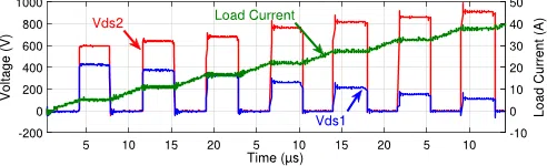
between two series-connected 1.2 kV SiC-MOSFETs is tested
in a pulse test setup. The experimental results confirm that the
proposed voltage balancing technique can drastically improve the
voltage sharing performance.
Index Terms—Series-Connection, SiC-MOSFETs, Gate Driver,
Parasitic Capacitances.
I. INTRODUCTION
T
HE energy transition with grid integration of distributed
energy resources, motor drive systems, and data cen-
ters leads to new challenges for power generation. Hence,
the medium-voltage grid and direct medium-voltage ap-
plications are becoming increasingly important. Medium-
voltage high-power converters have great potential for a
wide variety of medium-voltage applications, such as high-
voltage direct current (HVDC), medium-voltage direct current
(MVDC), smart/super/micro-grids, drives for electrical ma-
chines, medium-voltage pulse generators for plasma applica-
tions, etc [1]. The common characteristic of the mentioned
applications is the high voltage ratings and the search for
maximizing the efficiency and output power capability of these
critical systems, which can be achieved by increasing the
blocking voltage of the devices. To this end, advancements
in power electronic technology areas such as semiconductor
devices and converter topologies have been investigated to
improve the blocking voltage, power density, and efficiency,
which can lower overall system cost and electricity consump-
tion [2], [3].
Using series-connected devices is an attractive way for
reaching higher blocking voltage with low-voltage devices.
The authors are with the Grenoble Electrical Engineering Labora-
tory (G2Elab) – Universite Grenoble Alpes, Grenoble 38400, France,
and also with the Centre National de la Recherche Scientifique
(CNRS), Paris 75016, France (e-mail:Luciano-Francisco.Sousa-Alves, Van-
Sang.Nguyen, Pierre.Lefranc, jean-christophe.crebier, Pierre-Olivier.Jeannin,
Benoit.Sarrazin@g2elab.grenoble-inp.fr).
Manuscript received April 19, 2005; revised August 26, 2015.
According to a study carried out in [4], using individual semi-
conductors in series results in lower cost, higher efficiency,
and features better on-resistance and higher current density
than using a single higher voltage device. However, series
connection of power devices introduces multiple challenges
related to the breakdown voltage, switching speed and switch-
ing transition location unbalance problems across each power
device [5]–[8].
Substantial works have been done to analyze the causes of
the power device voltage unbalance, and several techniques
have been proposed to reduce this problem. The voltage
unbalance is mainly due to device’s parameters spread, gate-
drive delay time jitter and parasitic elements, especially the
one between each series connection potential and ground or
reference potential [9]–[12]. Passive snubber circuits [13]–
[17], active voltage clamping [18], [19], active gate control
[12], [20]–[23] and natural self-voltage balancing techniques
[10], [11], [24], [25], are used to improve the voltage sharing
performance.
Passive snubber circuits are a common method applied for
voltage balancing applications in industry due to its simple
design and implementation. However, in medium-voltage high-
frequency applications, passive methods lead to high power
loss due to the stress of higher dv/dt rates on the passive
components [26]. The cost and volume of the system can also
be increased due to the additional passive components in the
snubber circuits.
Active voltage clamping method is an effective way to
ensure an acceptable static voltage sharing across the devices.
However, the cost and volume of the system can be increased
due to the additional passive components in the clamp circuits.
Moreover, some methods require separate high-voltage rated
auxiliary voltage sources to clamp each driving voltage at the
desired voltage levels. Speed response can also become an
issue, especially when high speed power devices are used,
such as SiC devices.
Compared to passive techniques or voltage clamping meth-
ods, active gate control tends to provide less losses, and more
compact footprint. On the other hand, active gate controls are
more complex to be implemented.
The main idea of natural self-voltage balancing methods is
to work on the parasitic capacitances of the switching cell to
mitigate the voltage unbalancing across the series-connected
devices. In such a way, passive or active clamping techniques
can be sized down and ideally removed.
In [25], a compact series-connected SiC-MOSFET module
using a single external gate driver is proposed. The proposed

2
technique takes advantage of the layout capacitances related to
the gate terminals to improve the voltage sharing performance
and achieve the energy storage units. In [11], [27], a multi-
step packaging concept was introduced for series-connected
SiC-MOSFETs. The proposed natural self-voltage balancing
concept considers optimal dielectric isolation for each device
in the stack leading to a multi-step geometry. It has a signif-
icant impact on the parasitic capacitances introduced by the
packaging structure, which is responsible for voltage balancing
problems. However, the proposed package does not solve the
voltage balancing problems caused by the gate driver parasitic
elements. In such a way, the package is not sufficient since
the parasitic capacitance introduced by the gate drive circuitry
is one of the main causes of voltage unbalancing [10]. In the
experimental set-up, the authors use batteries to supply the
gate drivers, mitigating the effects of the parasitic capacitances
introduced by the gate drive power supplies. Furthermore, the
voltage sharing performance under different load conditions is
not analyzed.
Based on the study carried out in [11], a novel package
geometry is analyzed in this paper. The natural self-voltage
balancing technique takes advantage of parasitic capacitances
introduced by a new package geometry to compensate the
impacts of the parasitic capacitances introduced by gate drive
power supplies.
The paper is organized as follows. In Section II, theoretical
analyses are done to investigate the impact of the parasitic
capacitances introduced by the classical planar packaging
and gate drive circuits. Section III presents a novel concept
of packaging and explains how the proposed package can
improve the voltage balancing across the series-connected
SiC-MOSFETs. In Section IV, the proposed packaging is
experimentally validated. Section V presents the conclusions
of this paper.
II. IMPACT OF GATE DRIVER AND PACKAGING/LAYOUT
PARASITIC CAPACITANCES ON VOLTAGE SHARING
PERFORMANCE
A. Gate Drive Power Supply Parasitic Capacitance
In Fig. 1 is shown the classical gate drive circuitry where
are highlighted the parasitic capacitances introduced by DC-
DC power supplies (C
ps
) and signal transmission functions of
gate drivers (C
iso
). The parasitic capacitances C
ps
and C
iso
have the same dynamic influence on the system. However,
in the present work, it is considered that the capacitance
C
iso
is negligible in relation to C
ps
since in the experiments,
isolated signals are implemented by optical fibers. In Fig. 2 is
shown the parasitic elements of the gate drive power supply
and its connections, where Z
p
and Z
s
are, respectively, the
impedances on the primary and secondary sides of gate driver
isolation barriers. As can be seen, two reference potentials are
presented in classical switching cells [28], [29], i.e., the ground
or reference potential of the remote control circuit (GND) and
the reference potential of the power circuit (-VDC). Both GND
and -VDC are isolated from each other. Therefore, isolated
power converters are implemented in order to enable the
isolation dedicated to the power supply parts, and optocouplers
or optical fibers are used to isolate the paths for the control
signals. It is important to note that, for security reasons the
heatsink is usually attached to the reference potential of the
remote control circuit (GND), not to -VDC.
Cps
Gate Drive Power Supply
Gate
Signal
Optocoupler
Ciso
Buffer
Sn
Sn-1
+
-
-VDC
Fig. 1. Parasitic capacitances introduced by gate drive circuits.
Gate Driver
Insulation Barrier
Zs
HeatSink
GND
Sn
Sn-1
-VDC
GND
Zp
Cps
Fig. 2. Parasitic elements of the gate drive power supply and its connections.
Because of the high dv/dt during the switching transients,
high charge/discharge currents through the parasitic capacitors
C
ps
are generated. Such charge/discharge currents have the
same influence that the load and gate currents during the
switching transient, impacting the dynamic behaviors of the
series-connected SiC-MOSFETs [30].
B. Packaging/Layout Parasitic Capacitance
To analyze the influence of parasitic capacitances introduced
by the classical packaging/layout, a cross section of a simpli-
fied planar package and its main elements are shown in Fig. 3,
which includes a base-plate, a DBC substrate, and two vertical
series-connected SiC-MOSFETs. In terms of voltage balancing
and switching speed performances, the drain attached copper
trace to ground parasitic capacitance (C
pac
) introduced by
the packaging, is critical. This parasitic capacitance is a key
point in the voltage balancing analysis performed in this
work. As shown in Fig. 3, two series-connected devices are
considered in a traditional planar package. Therefore, two
parasitic capacitances (C
pac1
and C
pac2
) are introduced, which
represent the modeling of the copper traces attached to the
drain in relation to the baseplate.
In Fig. 4 is shown an electrical scheme of two SiC-
MOSFETs connected in series, where C
pac1
and C
pac2
are
the drain attached copper trace to ground (heatsink) parasitic
capacitances associated to the devices S1 and S2, respectively.
C
DC+
and C
DC−
are the parasitic capacitances from the DC

3
Cpac2
Cpac1
SiC DEVICES
INSULATING SUBSTRATE
PARASITIC CAPACITANCES
CASE
WIRE BONDS
BASEPLATE
S1 S2
Fig. 3. Cross-section of a simplified standard 2D planar package with two
dies connected in series.
bus to the ground, and C
Y
are the Y-capacitors often used
to suppress the EMI issues [31]–[33]. C
Y
are usually placed
between + VDC and GND, and - VDC and GND.
+VDC
Load
-VDC
S2
S1
HeatSink
Cpac1
Cpac2
CDC-
CDC+
GND
GND
CY
CY
Fig. 4. Equivalent electrical scheme of two SiC-MOSFETs connected in series
in a 2D planar package.
The capacitors C
pac1
and C
pac2
shown in Figs. 3 and 4 are
roughly all the same. However, the dv/dt applied to each of
them is different with respect to the position of the device in
the stack. Therefore, each parasitic capacitor carries a parasitic
current that is getting greater and greater with the device
number in the stack (starting from the bottom). The currents
that circulate through C
pac
can drastically impact the dynamic
behavior of SiC devices [34], [35]. The capacitors C
pac
can
be estimated based on the planar capacitance formula (1).
C
pac
=
A
d
(1)
Where is the absolute permittivity of the isolated substrate,
A is the area of the copper trace where the SiC device is
attached, and d is the distance between the copper plate and
the baseplate.
C. Impact of Parasitic Capacitances on Voltage Balancing
In Fig. 5 is shown the parasitic capacitance networks
introduced by the classical packaging (yellow zone) and
gate drive circuits (blue zone) for two series-connected SiC-
MOSFETs. The capacitances C
s
are the equivalent drain-
source intrinsic parasitic capacitances of devices, which are
considered all identical. As shown in Fig. 6, a high frequency
equivalent circuit can be achieved by short-circuiting the DC-
bus terminals and CY capacitors. As can be seen, two parasitic
+VDC
Load
-VDC
S2
Cpac1
Cpac2
CDC-
CDC+
GND
S1
Cs
Cs
GND
CY
Cps2
Cps1
CY
Gate Driver
Planar Package
Fig. 5. Equivalent electrical scheme of two SiC-MOSFETs connected in
series: 2D planar package and gate drive circuitry.
capacitance networks impact the voltage sharing performance,
i.e., the gate driver parasitic capacitance network (blue zone),
and the package/layout parasitic capacitance network (yellow
zone).
GND
Load
GND
S2
Cpac2
S1
Cs
Cs
Cpac1
GND
Cps2
Cps1
Icn2
Ips2
Ipac1
Ics2
Ics1
Icn1
Gate Driver
Planar Package
Fig. 6. High frequency equivalent electrical scheme of two series-connected
SiC-MOSFETs in a 2D planar package.
To prove that these parasitic capacitance networks unbal-
ance the voltages across series-connected SiC-MOSFETs, a
simple proof by contradiction can be done. Consider the cur-
rent distribution shown in Fig. 6, and the following equations:
I
cn2
+ I
cs2
= I
cn1
+ I
cs1
+ I
ps2
+ I
pac3
(2)
Where I
csi
is the current that flows through C
s
of the device
i, I
cni
is the channel current of the device i, I
ps2
is the
current that circulates through the gate driver capacitance C
ps2
and I
pac1
is the current that flows through package parasitic
capacitance C
pac1
.
Applying the proof by contradiction, it can be considered
that the V
ds
voltages across the devices are perfectly balanced.
Therefore, the following conditions can be applied:
• 1) the devices experiment equal drain-to-source dv
ds
/dt.
It implies that I
cs2
= I
cs1
= I
cs
since the devices are
considered identical.

4
• 2) the channel currents I
cn2
and I
cn1
are identical.
Applying these conditions to Eq. (2):
I
ps2
+ I
pac1
= 0 (3)
According to Eq. (3) and Fig. 6, the voltages across the
series-connected devices are perfectly balanced, if and only if,
I
pac1
= I
ps2
= 0. However, the greater is the switching speed
transition, the greater are I
pac1
and I
ps2
. In other words, in
a switching cell composed by SiC-MOSFET devices, these
currents are always greater than zero. Therefore, even if there
is no delay between the gate signals and no mismatch between
device characteristics, the V
ds
voltages will be unbalanced due
to the parasitic capacitances of gate driver and package/layout.
III. A NOVEL MULTI-STEP PACKAGING CONCEPT
To compensate the parasitic currents that flow into the gate
drive circuitry, a novel Multi-Step Packaging (MSP) concept
is proposed in this work. In Fig. 7 is shown the proposed
package, which has the following characteristics:
Cpac3
Cpac2
Cpac1
S2
S1
COPPER PLATES
ISOLATED SUBSTRATE
BASEPLATE
CASE
PARASITIC CAPACITANCES
GND
SiC DEVICES
Fig. 7. Novel Proposed Multi-Step Packaging.
• The parasitic capacitors introduced by the packaging
(C
pac
) are located between two subsequent copper layers.
• The devices are placed in the bottom-to-top direction
SN→...→S2→S1, where SN is the device connected to
the switching cell middle-point.
• For N devices connected in series, it is necessary to have
N+1 steps. As shown in Fig. 7, for two series-connected
devices, three steps are implemented. The third stage is
introduced to generate the parasitic capacitance C
pac1
between the drain attached bottom device and the ground.
• The number of parasitic capacitances introduced by the
packaging is equal to N+1. As shown in Fig. 7 for two
series-connected devices, three parasitic capacitances are
introduced.
In Fig. 8 is shown the electrical circuit configuration of the
parasitic capacitances of the proposed MSP geometry and gate
drive circuitry. The green zone represents the parasitic capaci-
tance network introduced by the MSP, where the capacitances
C
pac
are located between the drain and source terminals of
each device. The blue zone represents the gate driver parasitic
capacitance network.
As shown in Fig. 9, a high frequency equivalent circuit can
be achieved by short-circuiting the DC-bus terminals and C
Y
capacitors. The main idea of the proposed package/layout is
to modify the parasitic capacitance C
pac
values to compensate
the impact of the gate driver parasitic capacitors C
ps
. In this
case, the impacts of C
pac
and C
ps
will be nullified by each
other. To this end, consider that all the gate drivers in Fig. 9 are
+VDC
Load
S2
Cpac1
Cpac2
CDC-
CDC+
GND
S1
Cs
Cs
GND
CY
Cps2
Cps1
CY
-VDC
Cpac3
Gate Driver
MSP Package
Fig. 8. Equivalent electrical scheme of MSP packaging and gate drive
circuitry.
GND
Load
GND
S2
Cpac1
Cpac2
S1
Cs
Cs
Cps2
Cps1
GND
Cpac3
Gate Driver
MSP Package
Fig. 9. High frequency electrical scheme of MSP packaging and gate drive
circuitry.
identical, i.e., C
ps1
= C
ps2
= C
ps
. Therefore, the electrical
scheme shown in Fig. 9 can be simplified as shown in Fig.
10, where:
C
eq i
= C
s
+ C
paci
(4)
To find the appropriate values of C
pac
that compensate the
influence of capacitances C
ps
, it can be supposed that the
voltages across the series-connected devices in Fig. 10 are
perfectly balanced, and find the C
pac
values that ensure this
supposition. Based on this assumption, it can be considered
that 1) the SiC-MOSFET channel currents are identical, 2) the
drain potential of the device N experiments N -times the
dv
dt
of
the drain potential of the device S1 (bottom device) and 3) the
series-connected devices have the same drain-to-source
dv
ds
dt
.
Therefore, according to the mentioned considerations and the
current distribution shown in Fig. 10, the following equation