scispace - formally typeset
Search or ask a question
Proceedings ArticleDOI

A CMOS chip set for accurate pulsed time-of-flight laser range finding

TL;DR: A laser rangefinder device based on pulsed time-of-flight (TOF) distance measurement techniques was constructed and tested and is capable of measuring the time position, rise time and pulse width of incoming optical pulses with ps precision in the amplitude range of more than 1: 50 000.
Abstract: A laser rangefinder device based on pulsed time-of-flight (TOF) distance measurement techniques was constructed and tested. Key blocks of the system are the integrated receiver channel and the integrated time-to-digital converter (TDC) fabricated in a 0.35-um CMOS technology. The receiver-TDC chip set is capable of measuring the time position, rise time and pulse width of incoming optical pulses with ps precision in the amplitude range of more than 1: 50 000. The timing detection is based on leading edge detection in the receiver channel, and the amplitude-dependent timing error is compensated for by utilizing the multichannel TDC. A measurement distance of 100 m is achieved to a target with a reflectance of about 10% at the signal level of SNR = 6, with an optical output power and receiver aperture of 12 W and 18 mm, respectively.

Summary (2 min read)

I. INTRODUCTION

  • The time-of-flight (TOF) radars are typically based on either continuous wave (CW) phase comparison method or on the measurement of the transit time (ΔT) of a short laser pulse to an optically visible target and back to the receiver [1] .
  • Optical distance measurement principles have important advantages over microwave radars, for example.
  • Laser radars have found use in several industrial distance measurement applications, for example in proximity sensors and in positioning of tools, and in automotive applications such as velocity control [2] - [4] .
  • This measurement principle enables cm-level precision even with a single transmitted pulse to distances up to tens of meters to noncooperative targets.
  • The CMOS integrated receiver channel detects a weak optical echo and generates logic level timing signals for the multi-channel TDC, which measures the time intervals between the transmitted and received pulses as well as the pulse widths and rise times used for the timing walk error compensation [5] .

A. Receiver channel

  • An integrated receiver channel was implemented in a standard 0.35-µm CMOS technology [5] .
  • The timing comparator is triggered only when the received pulse exceeds a predetermined threshold voltage (Vth_L) which is related to the noise level of the receiver [7] as shown in Fig. 3 .
  • Unfortunately, the leading edge timing discrimination principle will produce a relatively large timing walk error (nanosecond range) in its basic configuration for the received optical echo whose amplitude varies a lot [8] .
  • It is only important to use the same threshold voltages for the calibration measurement (measurement of compensation tables) and for the actual distance measurement in which the compensation table is used.
  • The measured characteristics of the receiver channel are: a signal bandwidth of ~250 MHz, a transimpedance of ~100 kΩ, the input referred rms noise current of the receiver ~100 nA (Cin,total ~3 pF) and the power consumption of about 180 mW.

B. Time-to-digital converter

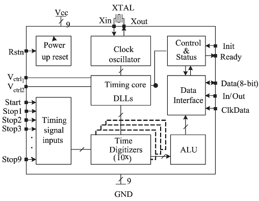
  • The multi-channel TDC circuit (10 parallel channels), composed of the blocks depicted in Fig. 5 , was fabricated in standard 0.35-µm CMOS process.
  • TDC solves time intervals accurately between the start and 3 timing signals from the receiver IC.
  • Δt1 defines an actual distance information (including walk error), Δt2-Δt1 corresponds to the pulse width and Δt3-Δt1 to the rise time information, used for the timing walk error compensation.
  • The multi-channel TDC (10 parallel channels) is based on a counter and delay line interpolation in two nested, different resolution levels.
  • One delay is divided into 32 LSB phases with parallel load capacitor-scaled delay elements [9] .

III. CONSTRUCTION AND MEASUREMENTS

  • The receiver channel, multi-channel TDC and laser transmitter were controlled using an Opal Kelly XEM6001 FPGA board.
  • In addition, the transmitter PCB consists of an ECL comparator (ADCMP553) which is used to generate a start signal for the TDC from the driving current of the laser diode.
  • The focal lengths of the transmitter and receiver optics are 30 mm and 20 mm, respectively.
  • The wide dynamic range for the reflected echo was achieved by using different kind of materials as the target.
  • This includes the jitter of the TDC (~10 ps), jitter induced by the compensation and the jitter of the receiver channel (due to noise).

IV. CONCLUSIONS

  • In conclusion, a CMOS chip-set was developed, fabricated and tested for a pulsed TOF laser radar.
  • In addition, the power consumption could be scaled down by using the shut-down principle while the laser transmitter is not operating.
  • The resulting dynamic range (1:1600) in [11] is narrower than in the proposed receiver.
  • It should be noted that the designed and measured receiver-TDC chip-set includes also the high performance time interval measurement unit which is in any case needed and is not shown in [11] , [12] .
  • The integrated receiver channel, multi-channel TDC and the time-domain walk compensation presented here, paves the way to miniaturized laser radar sensor systems.

Did you find this useful? Give us your feedback

Content maybe subject to copyright    Report

Citations
More filters
Journal ArticleDOI
TL;DR: The proposed phase division technique can be applied to not only the TDC but also the digital-to-time converter (DTC) to enrich its future applications and prove the superiority of the proposed structure to its stochastic counterparts.
Abstract: An extremely high-resolution, 2-D Vernier field-programmable gate array (FPGA) time-to-digital converter (TDC) with phase wrapping and averaging has been proposed recently to get an extremely fine resolution of 2.5 ps. However, the cell delays in a delay matrix are not fully controlled so that the TDC performance strongly depends on the stochastic distribution of cell delays, and the input range is limited to less than 20 ns. To achieve both high-precision phase division and wide measurement range, a phase-locked loop (PLL)-based delay matrix, which is capable of overclocking and double data rate (DDR), is proposed in this article. All delay cells are under the precise control of PLLs to generate output phases evenly divided within the reference clock period. For a concept proof, the TDC architecture is implemented on an Altera Stratix-IV FPGA chip to achieve 15.6-ps resolution. The differential nonlinearity (DNL), integral nonlinearity (INL), and rms resolution are measured to be merely −0.157 to 0.137 LSB, −0.176 to 0.184 LSB, and 1.0 LSB, which prove the superiority of the proposed structure to its stochastic counterparts. The proposed high-precision phase division technique can be applied to not only the TDC but also the digital-to-time converter (DTC) to enrich its future applications.

17 citations


Cites methods from "A CMOS chip set for accurate pulsed..."

  • ...physics, biomedical engineering, and time-of-flight measurement [1]–[3], TDCs are also applied in design-for-testability such as on-chip delay, temperature, and voltage measurements [4] and [5]....

    [...]

Journal ArticleDOI
TL;DR: An innovative autofocus method to ensure the image of an integrated circuit is correctly in focus under an infrared microscope is proposed and its robustness is tested using different magnifying lenses in addition to multiple distortions.
Abstract: This paper proposes an innovative autofocus method to ensure the image of an integrated circuit is correctly in focus under an infrared microscope. It discusses the difficulties inherent to the optical system and explores several inefficient methods used for natural scenes. It will also present a Focus Metric based on POlynomial Decomposition (FMPOD) adapted to our context. This approach relies on analyzing the projection of images on an orthonormal polynomial basis. Its robustness is tested using different magnifying lenses in addition to multiple distortions. In conclusion, we will demonstrate how this novel approach outperforms existing methods related to our work environment.

3 citations


Cites background from "A CMOS chip set for accurate pulsed..."

  • ...A recent technology based on time-of-flight camera creates a complete depths map of a scene, or more precisely a map of each pixel of the camera sensor [3], [4]; innovations in this technology are still being studied [5]....

    [...]

Journal ArticleDOI
TL;DR: In this paper, the authors proposed a new telemeter scheme for absolute distance measurements, based on a semiconductor ring laser, working in the bistability regime, which combines time-of-flight and optical injection, is very simple to implement, since, in addition to the laser, it only requires mirrors and collimation or focusing optics.
Abstract: We propose a new telemeter scheme for absolute distance measurements, based on a semiconductor ring laser, working in the bistability regime. The optical feedback provided by two external reflectors (a fixed one at short distance, and a moveable one defining the measuring arm) generates commutations of the propagation direction (clockwise, counter-clockwise) inside the ring laser, the period of which is linearly related to the distance of the measure arm reflector. A convenient electrical output signal can be easily obtained by a photodiode located behind the (partially reflecting) fixed mirror. This telemeter, which combines time-of-flight and optical injection, is very simple to implement, since, in addition to the laser, it only requires mirrors and collimation or focusing optics. Also electronic driving and processing are straightforward. Differently from most time-of-flight telemeters, this scheme does not require special provisions or processing to tackle the ambiguity problem. Simulations are performed by mathematical models based on rate-equations. This telemeter has been evaluated in the range 10 cm–32 m of round trip distance, with a fixed arm of 10 μm–10 cm, assuming typical literature parameters for a 1 mW ring laser.
1 citations

Patent
26 Nov 2019
TL;DR: In this article, the authors proposed a radar signal real-time detection method, which is characterized by comparing an average amplitude of N sampling points before a certain moment with the amplitude of the sampling point at the moment.
Abstract: The invention relates to a radar signal real-time detection method. The method is characterized by comparing an average amplitude of N sampling points before a certain moment with the amplitude of thesampling point at the moment, and if the amplitudes of the plurality of sampling points after starting of the certain moment are continuously a certain value higher than the average amplitude in a previous certain period of time, considering that a signal rising edge exists at the moment; otherwise, if the amplitudes of the plurality of continuous sampling points after a certain moment is startedare a certain value lower than the previous average amplitude, considering that a falling edge exists at the moment; and when both the falling edge and the rising edge exist, intercepting a signal part existing in data immediately. Whether a signal exists is detected in a mode of judging the rising edge and the falling edge in a time domain, and an effect of detecting the signal in real time under a passive condition can be achieved by setting reasonable parameters and thresholds.
References
More filters
Proceedings ArticleDOI
15 Dec 2014
TL;DR: In this article, a compact laser pulser emitting ∼100 ps, ∼10 W pulses at >100 kHz is presented, where the high pulsing frequency is achieved using a MOSFET-based current driver, whereas the high pulse power is a merit of the used laser diode with an asymmetric waveguide structure leading to enhanced gain switching.
Abstract: A compact laser pulser emitting ∼100 ps, ∼10 W pulses at >100 kHz is presented. The high pulsing frequency is achieved using a MOSFET-based current driver, whereas the high pulse power is a merit of the used laser diode with an asymmetric waveguide structure leading to enhanced gain switching. The pulsing frequency is higher than with avalanche transistor based current pulsing circuits due to lower heating, and the current pulse width is shown to be even shorter than with avalanche transistor based circuits. The laser diode transmitter was developed especially for the pulsed time-of-flight laser radar application utilizing a single photon avalanche diode (SPAD) matrix as the detector element. A demonstration measurement is done enabling centimeter-precision distance measurement to 50 m in a measurement time of ∼5 ms outdoors in sunny weather.

25 citations


"A CMOS chip set for accurate pulsed..." refers methods in this paper

  • ...The transmitter consists of a laser diode (905D1S2J03Y from Laser Components) and a laser diode driver, which was realized with a MOS switch and an LRC transient-based pulse shape control [10]....

    [...]

Journal ArticleDOI
TL;DR: As researchers and developers finesse the next generation of gaming consoles and devices, everything is coming up 3-D, and consumers are “virtually” salivating.
Abstract: As researchers and developers finesse the next generation of gaming consoles and devices, everything is coming up 3-D, and consumers are “virtually” salivating.

14 citations


"A CMOS chip set for accurate pulsed..." refers background in this paper

  • ...The high level of integration paves the way for low-cost, and miniaturized LIDAR sensors, which are needed in emerging new applications [6]....

    [...]

Frequently Asked Questions (1)
Q1. What have the authors contributed in "A cmos chip set for accurate pulsed time-of- flight laser range finding" ?

In this paper, a laser rangefinder device based on pulsed time-of-flight ( TOF ) distance measurement techniques was constructed and tested.