scispace - formally typeset
Search or ask a question
Proceedings ArticleDOI

A Comparative Study of Proton Radiation Damage in p- and n-Channel CCDs

20 Aug 2009-Proceedings of SPIE (International Society for Optics and Photonics)-Vol. 7435, pp 95-102
TL;DR: In this paper, a comparative study of n-channel and p-channel charge coupled devices (CCDs) was conducted under the same conditions, and it was shown that p-CCDs are more radiation hard than conventional nchannel devices as they are not affected by the dominant electron trapping caused by the displacement damage defect the phosphorus-vacancy.
Abstract: It has been demonstrated that p-channel charge coupled devices (CCDs) are more radiation hard than conventional nchannel devices as they are not affected by the dominant electron trapping caused by the displacement damage defect the E-centre (phosphorus-vacancy). This paper presents a summary of the results from a comparative study of n-channel and p-channel CCDs each type operated under the same conditions. The CCD tested is the e2v technologies plc CCD47-20, a 1024 × 1024 frame transfer device with a split output register, fabricated using the same mask to form n-channel and p-channel devices. The p-channel devices were irradiated to a 10 MeV equivalent proton fluence of 4.07×10 10 protons.cm -2 and 1.35×10 11 protons.cm -2 , an n-channel CCD was irradiated to a 10 MeV equivalent proton fluence of 1.68×10⁹ protons.cm-2, however due to time constraints the n-channel device was not characterised, n-channel comparisons are instead made using a CCD02. As expected the p-channel CCD demonstrated improved radiation tolerance when compared to the n-channel CCD, at -90 °C there is an approximate ×7 and ×15 improvement in tolerance to radiation induced parallel and serial CTI respectively for equivalent pixel geometries.

Summary (2 min read)

1. INTRODUCTION

  • The concentration of phosphorous is two orders of magnitude lower than that in n-channel devices; therefore the formation of E-centre defects will be negligible [5].
  • The parallel and serial buried channel widths are 17.5 µm and 36.0 µm respectively.
  • The image area was irradiated leaving the store region un-irradiated to act as a control, serial CTI would not be measured as the serial register was not irradiated.
  • The entire active area of six p-channel devices and one n-channel device were irradiated using 63 MeV protons at the Paul Scherrer Institut (PSI) in Switzerland, with one n-channel and p-channel device held as a control.

2. EXPERIMENTAL ARRANGEMENT

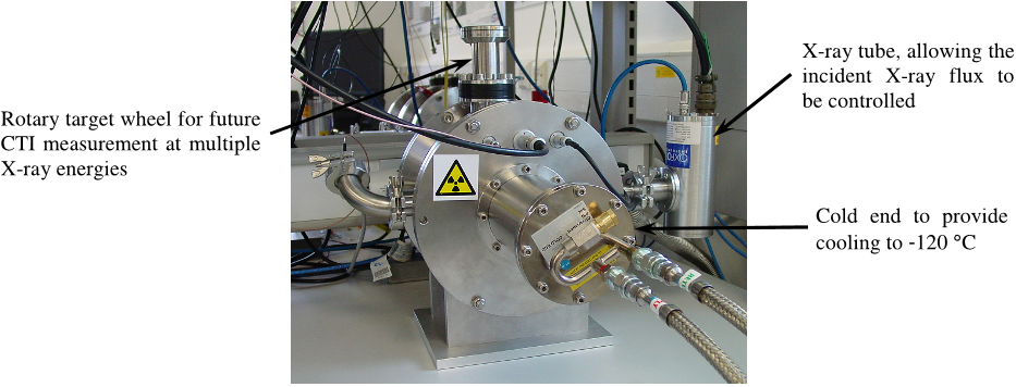
  • The CCD47 was housed inside the vacuum test facility shown in Figure 2.
  • Initially a potential mirror was created to convert the potentials provided by the XCAM Ltd. USB2REM1 camera drive box to those required to operate the p-channel CCD, given in Table 2.
  • Mirroring the clock and reset potentials introduced a large amount of additional system noise, therefore, the mirror on the clock and reset potentials was removed and the ground referenced to 12.0 V to provide the required potentials.

3.1 Dark Current

  • The mean dark current was measured across the surface of the p-channel devices using six sets of images, each taken using a 30 s integration period, the results as a function of temperature for three of the devices are shown in Figure 3.
  • Srour demonstrated that a trap with an activation energy of 0.63 eV, attributed to the divacancy, is responsible for the temperature dependence of dark current associated with thermally generated charge [6].
  • The data were plotted in an Arrhenius plot, shown in Figure 4, with a line of best fit drawn through data points above -55 °C.
  • The feature formed below -90 °C is believed to show the limit of the measurement technique, where insufficient dark current is generated to be measured, requiring a longer integration period.

3.2 Charge Transfer Inefficiency

  • The initial testing was performed using the p-channel control CCD held at -110.0 °C using an X-ray density of one event per 700 pixels, conducting fifteen readouts in 10 °C intervals, the results for parallel CTI are displayed in Figure 4.
  • To increase the rate of data collection and the number of data points the X-ray density was increased to one event per 250 pixels, requiring only six readouts taken at 5 °C intervals, the results for parallel CTI are displayed in Figure 5.
  • The temperature dependence of parallel CTI pre and post irradiation is shown in Figure 6, the trend for the irradiated and un-irradiated devices both demonstrate an increase in CTI as the device is cooled, possibly due to removal of thermally generated charge keeping the traps filled.
  • The slow parallel line transfer, at 50 kHz, does not benefit from the increased emission time.
  • The p-channel CCDs tested exhibited comparable parallel CTI, however, the serial CTI varied between the un-irradiated device and devices irradiated with the same proton fluence, as illustrated in Figure 7 where the CTI of a CCD irradiated with 4.07×10¹⁰ protons.cm-2 was measured to be lower than the un-irradiated control.

4. CONCLUSIONS

  • The p-channel CCD47s tested demonstrate a clear improvement in tolerance to radiation induced CTI, showing an improvement of ×7 and ×15 for parallel and serial CTI respectively for equivalent pixel geometries when compared to an n-channel CCD.
  • A program is required to improve the base parallel and serial CTI, possibly through the use of a bulk (float zone) devices which have demonstrated base CTI equivalent to n-channel devices, demonstrated by Bebek et. al. [7] and Dawson et. al. [11].
  • Unfortunately the devices were not available for testing prior to the irradiation so no comparison could be made on the rate of hot pixel generation.
  • The potential mirror will also be developed to improve its noise performance.

Did you find this useful? Give us your feedback

Content maybe subject to copyright    Report

Open Research Online
The Open University’s repository of research publications
and other research outputs
A comparative study of proton radiation damage in p-
and n-channel
Conference or Workshop Item
How to cite:
Gow, J.; Murray, N. J.; Holland, A. D.; Burt, D. and Pool, P. (2009). A comparative study of proton radiation damage
in p- and n-channel. In: Proceedings of SPIE: UV, X-Ray, and Gamma-Ray Space Instrumentation for Astronomy
XVI, 3 Aug 2009, San Diego, USA.
For guidance on citations see FAQs.
c
SPIE - The International Society for Optical Engineering
Version: Accepted Manuscript
Link(s) to article on publisher’s website:
http://dx.doi.org/doi:10.1117/12.826866
Copyright and Moral Rights for the articles on this site are retained by the individual authors and/or other copyright
owners. For more information on Open Research Online’s data policy on reuse of materials please consult the policies
page.
oro.open.ac.uk

A Comparative Study of Proton Radiation Damage in p- and n-
Channel CCDs
J. Gow*
a
, N. J. Murray
a
, A. D. Holland
a
, D. Burt
b
, P. Pool
b
a
e2v centre for electronic imaging, The Open University, PSSRI, Milton Keynes, MK7 6AA, UK
b
e2v technologies plc, 106 Waterhouse Lance, Chelmsford, Essex, CM1 2QU, UK
ABSTRACT
It has been demonstrated that p-channel charge coupled devices (CCDs) are more radiation hard than conventional n-
channel devices as they are not affected by the dominant electron trapping caused by the displacement damage defect the
E-centre (phosphorus-vacancy). This paper presents a summary of the results from a comparative study of n-channel and
p-channel CCDs each type operated under the same conditions. The CCD tested is the e2v technologies plc CCD47-20, a
1024
×
1024 frame transfer device with a split output register, fabricated using the same mask to form n-channel and
p-channel devices. The p-channel devices were irradiated to a 10 MeV equivalent proton fluence of 4.07
×
10
10
protons.cm
-2
and 1.35
×
10
11
protons.cm
-2
, an n-channel CCD was irradiated to a 10 MeV equivalent proton fluence of
1.68
×
10
9
protons.cm
-2
, however due to time constraints the n-channel device was not characterised, n-channel
comparisons are instead made using a CCD02. As expected the p-channel CCD demonstrated improved radiation
tolerance when compared to the n-channel CCD, at -90 °C there is an approximate ×7 and ×15 improvement in tolerance
to radiation induced parallel and serial CTI respectively for equivalent pixel geometries.
Keywords: CCD, Proton radiation damage, p-channel, n-channel, charge transfer efficiency, displacement damage
hardened
1. INTRODUCTION
The work presented in this paper has been carried by the e2v centre for electronic imaging at the Open University to
investigate the post proton irradiation performance of n-channel and p-channel CCDs fabricated using the same mask set.
It is essential for a space mission that the selected detector meets the performance requirements over the mission
duration, accounting for performance loss due to the space radiation environment [1]. Displacement damage caused by
protons within the Earths radiation belts and from cosmic rays (solar and galactic) generate stable lattice defects within
the silicon, creating energy levels within the silicon band-gap. The three main stable defects, for n-channel CCDs, are the
phosphorous vacancy (E-centre) at 0.44 eV, the oxygen-vacancy (A-centre) at 0.18 eV (both as a result of impurity
atoms within the lattice), and the divacancy (J-centre) at 0.40 eV and 0.25 eV consisting of two adjacent vacancies. The
E-centre is located at near mid-gap, the ideal location for electron trapping. An n-channel device uses phosphorus as the
dopant atom for the buried channel; it was suggested and demonstrated that using boron to create a p-channel device
would reduce the post irradiation increase in charge transfer inefficiency (CTI) [2].
It is difficult to compare CTI results taken using different operating conditions and equipment setups, as described
elsewhere in this volume [3]. The aim of this work was to provide a definitive comparison of n-channel and p-channel
devices. The devices were to be operated using the same drive voltages and timings, held in the same position within the
test facility and exposed to the same incident X-ray flux, however due to time constraints the n-channel CCD47 was not
tested. Results found using a CCD02 characterised using comparable voltages, timings, and X-ray flux [4] were used to
provide the n-channel comparison. The X-ray method was selected as the measurement technique for CTI, using Mn-K
α
X-rays at 5,898 eV (
~
1600 e
-
), measured between -40.0 °C and -110.0 °C, with the dark current measured between
0.0 °C and -110.0 °C.
*jpdg3@open.ac.uk; phone +44 (0) 1908 852 769; fax +44 (0) 1908 858 052; www.open.ac.uk/cei

The CCD tested was the e2v technologies plc front illuminated CCD47-20, a frame transfer device with an image and
store format of 1024 by 1024 with 13 µm square pixels, illustrated in Figure 1a. The parallel and serial buried channel
widths are 8.5 µm and 24.0 µm respectively. The p-type buried channel was doped with boron, the epitaxial layer with
phosphorous (20 to 100 .cm), and the substrate with antimony (< 20 m.cm). The dopants were selected to provide
comparable resistivity and properties to those found in n-channel devices, for ease of manufacture [5]. The concentration
of phosphorous is two orders of magnitude lower than that in n-channel devices; therefore the formation of E-centre
defects will be negligible [5]. The CCD02 is a front illuminated device, with an image format of 385 by 578 with 22 µm
square pixels, illustrated in Figure 1b. The parallel and serial buried channel widths are 17.5 µm and 36.0 µm
respectively.
Fig. 1. A photograph of the p-channel CCD47-20 [a] and the n-channel CCD02 [b]
A proton irradiation was originally conducted, using two p-channel devices and one n-channel device, at the Kernfysisch
Versneller Instituut (KVI) in the Netherlands. The image area was irradiated leaving the store region un-irradiated to act
as a control, serial CTI would not be measured as the serial register was not irradiated. A pre-irradiation characterisation
was not performed and post-irradiation it became apparent that the irradiated devices, and un-irradiated devices from the
same wafer, exhibited defects which flooded the active area with excess charge. As a result testing moved to six
p-channel devices which had been irradiated as part of an e2v study into p-channel and n-channel devices, funded by
ESA. The entire active area of six p-channel devices and one n-channel device were irradiated using 63 MeV protons at
the Paul Scherrer Institut (PSI) in Switzerland, with one n-channel and p-channel device held as a control. The irradiation
details, including the 10 MeV proton fluence, is summarised in Table 1. Post irradiation an anneal stage at 100 °C, with
the irradiated devices unbiased, was performed for a duration of 168 hours the p-channel devices exhibited negligible
change in CTI post anneal [5].
Table 1. Irradiation Characteristics for p-channel and n-channel CCD47-20s
Device Type
Beam Energy
(MeV)
Flux
(p.cm
-2
.s
-1
)
Fluence
(p.cm
-2
)
10 MeV equivalent
fluence (p.cm
-2
)
×3 p-channel 63 1.70×10
8
2.70×10
11
1.35×10
11
×3 p-channel 63 1.40×10
8
8.12×10
10
4.07×10
10
×1 p-channel Not irradiated
×1 n-channel 44 1.95×10
7
3.03×10
9
1.68×10
9
×1 n-channel Not irradiated
2. EXPERIMENTAL ARRANGEMENT
The CCD47 was housed inside the vacuum test facility shown in Figure 2. A vacuum pump was used to evacuate the air
in the chamber with testing occurring at a pressure of < 10
-5
mbar. The CCD being tested was clamped onto a copper
cold bench connected to a CryoTiger® refrigeration system (PT-30) capable of cooling the detector to around -120 °C or
153 K. A resistive heater was employed in thermal contact between the copper cold bench, allowing a maximum
operating temperature of -40 °C before overloading the cooling capacity of the CryoTiger®. To allow for warmer
operating temperatures the data were recorded as the CCD cooled, with the heater at maximum to reduce the cool down
rate. The temperature can be controlled to within ± 0.1 °C using a feedback system, comprising a Lakeshore 325
temperature controller, platinum resistance thermometer (PRT), and the heater. The temperature of the CCD ceramic was
[a] [b]

measured using a 1,000 PRT (it is assumed the device silicon is in good thermal contact with the ceramic). An Oxford
Instruments XTF5011/75-TH X-ray tube (tungsten anode) was used to fluoresce a manganese target held at 45° to the
incident X-ray beam to provide a known energy (5,898 eV) for calibration and CTI measurements, with an X-ray density
of approximately one event every two hundred and fifty pixels.
Fig. 2. A photograph of the vacuum test facility
Initially a potential mirror was created to convert the potentials provided by the XCAM Ltd. USB2REM1 camera drive
box to those required to operate the p-channel CCD, given in Table 2. Mirroring the clock and reset potentials introduced
a large amount of additional system noise, therefore, the mirror on the clock and reset potentials was removed and the
ground referenced to 12.0 V to provide the required potentials. The total noise measured at -110 °C reduced from 200 e
-
r.m.s. to 20 e
-
r.m.s after the removal of the potential mirror. A headboard provided local low-pass filtering for the D.C.
bias connections and pre-amplification of the output, with the clocking and biasing provided by an XCAM Ltd.
USB2REM1 camera drive box in conjunction with USB2 v1.15 drive software. The devices were operated using a line
transfer rate of 50 kHz, and a readout rate of 500 kHz.
Table 1. CCD47-20 operational voltages
Clock/Bias Description Bias Used (V)
Vss Substrate 0.0
Vog Ouput gate 3.0
Vrd Reset drain 17.0
Vod Output drain 32.0
Image/Store clock 12.0
Register clock 12.0
ØR Reset gate 12.0
V
ABD
Anti blooming drain 28.0
3. RESULTS AND DISCUSSIONS
3.1 Dark Current
The mean dark current was measured across the surface of the p-channel devices using six sets of images, each taken
using a 30 s integration period, the results as a function of temperature for three of the devices are shown in Figure 3.
Srour demonstrated that a trap with an activation energy of 0.63 eV, attributed to the divacancy, is responsible for the
temperature dependence of dark current associated with thermally generated charge [6]. The data should be proportional
to exp(-0.63/kT), where k is Boltzmann’s constant and T is the temperature. The data were plotted in an Arrhenius plot,
Rotary target wheel for future
CTI measurement at multiple
X-ray energies
X-ray tube, allowing the
incident X-ray flux to
be controlled
Cold end to provide
cooling to -120 °C

shown in Figure 4, with a line of best fit drawn through data points above -55 °C. The feature formed below -90 °C is
believed to show the limit of the measurement technique, where insufficient dark current is generated to be measured,
requiring a longer integration period. The activation energy was calculated to be 0.61 eV un-irradiated, 0.62 eV
irradiated with 4.07×10
10
protons.cm
-2
, and 0.63 eV irradiated with 1.35×10
11
protons.cm
-2
, the results are comparable to
those found by Srour [6], Bebek et. al. [7], and Spratt [8]. This suggests that for the p-channel devices tested the
divacancy is the dominant source of thermally generated dark current pre and post irradiation. The increase in dark
current as a function of proton fluence is approximately linear. Based on the fits to the data the increase after irradiation
at 21 °C (at this temperature the device was saturated i.e. ADC max out) was calculated to be
~
1.4 nA.cm
-2
.krad
-1
,
similar to that found in the p-channel CCD02 [9] and other e2v n-channel CCDs [10].
Fig. 3. Dark current as a function of temperature for three p-channel devices pre and post irradiation
Fig. 4. Dark current as a function of 1000/T for three p-channel devices pre and post irradiation
0.01
0.1
1
10
100
1000
3.7 3.9 4.1 4.3 4.5 4.7 4.9 5.1 5.3 5.5 5.7
1000/T (1000.K
-1
)
Dark Current (e
-
.pixel
-1
.s
-1
)
Series4
2.70E+11
Series5
Un-Irrad
Series6
8.12E+10
Expon. (2.70E+11)
Un-irradiated control
4.07×10
8
p.cm
-2
1.35×10
8
p.cm
-2
Best fit to un-irradiated data
Best fit to 4.07×10
10
p.cm
-2
data
Best fit to 1.35×10
11
p.cm
-2
data
Limit of measurement
technique
1
10
100
1000
-75.0 -70.0 -65.0 -60.0 -55.0 -50.0 -45.0 -40.0 -35.0 -30.0
Temperature (
o
C)
Dark Current (e
-
.pixel
-1
.s
-1
)
Series4 8.12E+10
Series5 2.70E+11
Series6 Un-Irrad
Series7 Expon. (Un-Irrad)
Expon. (8.12E+10) Expon. (2.70E+11)
Un-irradiated control
4.07×10
8
p.cm
-2
1.35×10
8
p.cm
-2
Best fit to un-irradiated data
Best fit to 4.07×10
10
p.cm
-2
data
Best fit to 1.35×10
11
p.cm
-2
data

Citations
More filters
Journal ArticleDOI
TL;DR: In this article, the effects of radiation-induced charge transfer inefficiency (CTI) in the Euclid CCDs over the course of the 5-year mission at L2 are understood.
Abstract: Euclid is a medium class European Space Agency mission candidate for launch in 2019 with a primary goal to study the dark universe using the weak lensing and baryonic acoustic oscillations techniques. Weak lensing depends on accurate shape measurements of distant galaxies. Therefore it is beneficial that the effects of radiation-induced charge transfer inefficiency (CTI) in the Euclid CCDs over the course of the 5 year mission at L2 are understood. This will allow, through experimental analysis and modelling techniques, the effects of radiation induced CTI on shape to be decoupled from those of mass inhomogeneities along the line-of-sight. This paper discusses a selection of work from the study that has been undertaken using the e2v CCD204 as part of the initial proton radiation damage assessment for Euclid. The experimental arrangement and procedure are described followed by the results obtained, thereby allowing recommendations to be made on the CCD operating temperature, to provide an insight into CTI effects using an optical background, to assess the benefits of using charge injection on CTI recovery and the effect of the use of two different methods of serial clocking on serial CTI. This work will form the basis of a comparison with a p-channel CCD204 fabricated using the same mask set as the n-channel equivalent. A custom CCD has been designed, based on this work and discussions between e2v technologies plc. and the Euclid consortium, and designated the CCD273.

28 citations

Proceedings ArticleDOI
TL;DR: In this paper, the authors report on the present and future detector development activities for the European Space Agency Science Programme (ESAP) in particular targeting large format and p-channel CCD, NIR and MWIR, LWIR wavelength ranges as well as related ASIC controller.
Abstract: We report on the present and future detector development activities for the European Space Agency Science Programme. The development of European technology in that field is a key mission enabler for the program, which requires TRL6 (ISO scale) by end of the definition phase, so called "mission adoption". This is particularly true for Astronomy and fundamental physics type missions. Current activities are in particular targeting large format and p-channel CCD, NIR and MWIR, LWIR wavelength ranges as well as related ASIC controller. For the longer term future mission plan (so called M4, M5 and L2 missions, M3 being PLATO and L1 JUICE), the extreme ends of the spectrum will be addressed. An overview of the detector status for the Earth Observation program is given in appendix, as most of the technologies are directly applicable to some extent to science missions, in particular for Planetary missions. The specific validation activities in place in the future mission preparation office in support to the space science program will be eventually briefly detailed.

11 citations

DissertationDOI
01 Jan 2016
TL;DR: In this paper, a method of physically modelling charge collection within the detector using analytical solutions to Poisson's equation is described, which is shown to qualitatively reproduce many features of measured dynamic charge collection effects.
Abstract: The subject of this thesis is the analysis of instrumental effects caused by the interaction between collected signal charge and electric fields within precision CCD imaging sensors typically used for astronomy. These phenomena cause aberrations in the measured spatial distribution of subsequently collected signal, which may present a major error for upcoming astronomy projects which rely heavily on accurately determining shapes of compact sources. Examples are the Large Synoptic Survey Telescope and the Euclid space telescope. The size of dynamic collection effects may be subtly affected by the operating conditions and design parameters of the device. Dynamic charge collection effects differ in origin from many other errors introduced by imaging detectors in that they are attributable to changes in the confinement of charge carriers during the collection phase of operation, rather than the readout phase. The fact that the exact aberration implied by dynamic charge collection effects depends exactly on the incident light field’s spatial distribution also makes them comparatively difficult to correct for. A method of physically modelling charge collection within the detector using analytical solutions to Poisson’s equation is described, which is shown to qualitatively reproduce many features of measured dynamic charge collection effects. Since the model is derived from device physics, it differs in approach in a complementary way from previous efforts which are empirically based. Experimental charge collection measurements from two different CCDs both affected by dynamic collection effects are presented, and shown in large part to be consistent with the predictions from the theoretical model.

7 citations


Cites background from "A Comparative Study of Proton Radia..."

  • ...On the other hand, there is also mounting evidence th a t p-channel devices may have some other im portant advantages in term s of radiation damage performance in space environments, due to the differing nature of traps present in n-type as compared with p-type silicon [36]....

    [...]

Proceedings ArticleDOI
07 Oct 2014
TL;DR: In this article, the authors present a study conducted during the Sentinel-4/UVN CCD pre-development to provide a first assessment of the radiation-induced charge transfer efficiency (CTI) effects on the Sentinel4 measurements.
Abstract: Energetic particles in space damage electronic components, and in particular affect the capability of Charge-Coupled Devices (CCD) to transfer photo-generated charge packets to the output node. If not properly accounted for either during the instrument design process or in the mission data processing pipeline, radiation-induced Charge Transfer Inefficiency (CTI) causes image distortion, decreases the signal-to-noise ratio, and ultimately leads to bias in the measurement carried out. CTI is a well-identified error budget contributor for mission operating in the photon-starving regime like space telescopes dedicated to Astronomy, but is less studied in the context of Earth Observation missions. We present a study conducted during the Sentinel-4/UVN CCD pre-development to provide a first assessment of the CTI effects on the Sentinel-4 measurements.

6 citations


Cites background from "A Comparative Study of Proton Radia..."

  • ..., [22, 23, 24]) instead of the more conventional n-type doped buried channel....

    [...]

Proceedings ArticleDOI
TL;DR: The International X-ray Observatory (IXO) project is the result of a merger between the NASA Con-X and ESA/Jaxa XEUS mission concepts.
Abstract: The International X-ray Observatory (IXO) project is the result of a merger between the NASA Con-X and ESA/Jaxa XEUS mission concepts. The IXO mission outline has an X-ray grating spectrometer operating in the 0.3-1 keV band. CCDs are the ideal detector for the readout of the grating spectrometer instrument and have been flown in similar functions on XMM and Chandra. Here we review the Off-Plane X-ray Grating Spectrometer concept for IXO and discuss the optimization of CCD technology for detection in the 0.2-2 keV X-ray band. We will discuss improvements to the existing technology previously flown, and the use of new technology such as electron multiplying CCDs which can provide enhanced signal to noise at these soft X-ray energies, together with radiation hardening measures and methods of reducing sensitivity to optical stray light. We will also end by discussing alternative CMOS-based technology which may be developed in future years to replace the CCD technology, offering benefits of higher system integration and radiation hardness.

3 citations

References
More filters
Journal ArticleDOI
01 Nov 1988
TL;DR: In this article, the Earth's space radiation environment is described in terms of charged particles as relevant to effects on spacecraft electronics, and the nature and magnitude of the trapped and transiting environments are described by spatial distribution and temporal variation.
Abstract: The Earth's space radiation environment is described in terms of charged particles as relevant to effects on spacecraft electronics. The nature and magnitude of the trapped and transiting environments are described in terms of spatial distribution and temporal variation. The internal radiation environment of the spacecraft is described in terms of shielding the high-energy particles of the free-field environment. Exposure levels are presented in terms of ionizing radiation dose and particle fluence for comparison to electronic component susceptibility. >

331 citations


"A Comparative Study of Proton Radia..." refers background in this paper

  • ...It is essential for a space mission that the selected detector meets the performance requirements over the mission duration, accounting for performance loss due to the space radiation environment [1]....

    [...]

Journal ArticleDOI
TL;DR: In this paper, basic mechanisms and ground-test data for radiation effects in solid-state imagers are reviewed, with a special emphasis on proton-induced effects on silicon charge-coupled devices (CCDs).
Abstract: Basic mechanisms and ground-test data for radiation effects in solid-state imagers are reviewed, with a special emphasis on proton-induced effects on silicon charge-coupled devices (CCDs). For the proton fluxes encountered in the space environment, both transient ionization and displacement damage effects arise from single-particle interactions. In the former case, individual proton tracks will be seen; in the latter, dark-current spikes (or hot pixels) and trapping states that cause degradation in charge-transfer efficiency will be observed. Proton-induced displacement damage effects on dark current and charge transfer are considered in detail, and the practical implications for shielding, device hardening, and ground testing are discussed.

189 citations


"A Comparative Study of Proton Radia..." refers background in this paper

  • ...krad, similar to that found in the p-channel CCD02 [9] and other e2v n-channel CCDs [10]....

    [...]

  • ...krad at 21 °C, was found to be comparable with other e2v n-channel CCDs [10]....

    [...]

Journal ArticleDOI
J.R. Srour1, D.H. Lo
TL;DR: In this paper, a new damage factor for describing radiation-induced dark current in silicon devices is presented. But the authors do not specify the defects responsible for the dark current increases.
Abstract: A new damage factor formulation is presented for describing radiation-induced dark current in silicon devices. This damage factor, K/sub dark/, is the number of carriers thermally generated per unit volume per unit time in a depletion region per unit nonionizing dose deposited in that volume. K/sub dark/ appears to account successfully for the mean radiation-induced dark current for any silicon device in which thermal generation at bulk centers dominates. This dark-current damage factor applies for devices in all radiation environments except those that produce relatively isolated defects. Evidence is presented which strongly indicates that the defects responsible for dark current increases are not associated with impurities.

133 citations


"A Comparative Study of Proton Radia..." refers background or result in this paper

  • ...cm, the results are comparable to those found by Srour [6], Bebek et....

    [...]

  • ...The activation energy was calculated to be 0.61 eV un-irradiated, 0.62 eV irradiated with 4.07×10¹⁰ protons.cm-2, and 0.63 eV irradiated with 1.35×10¹¹ protons.cm-2, the results are comparable to those found by Srour [6], Bebek et. al....

    [...]

  • ...Srour demonstrated that a trap with an activation energy of 0.63 eV, attributed to the divacancy, is responsible for the temperature dependence of dark current associated with thermally generated charge [6]....

    [...]

  • ...63 eV, attributed to the divacancy, is responsible for the temperature dependence of dark current associated with thermally generated charge [6]....

    [...]

Journal ArticleDOI
04 Nov 2001
TL;DR: P-channel backside illuminated silicon charge-coupled devices (CCDs) were developed and fabricated on high-resistivity n-type silicon as discussed by the authors, which have been exposed up to 1 /spl times/ 10/sup 11/ protons/cm/sup 2/ at 12 MeV.
Abstract: P-channel backside illuminated silicon charge-coupled devices (CCDs) were developed and fabricated on high-resistivity n-type silicon. The devices have been exposed up to 1 /spl times/ 10/sup 11/ protons/cm/sup 2/ at 12 MeV. The charge transfer efficiency and dark current were measured as a function of radiation dose. These CCDs were found to be significantly more radiation tolerant than conventional n-channel devices. This could prove to be a major benefit for space missions of long duration.

56 citations

Journal ArticleDOI
TL;DR: In this paper, an experimental batch of p-buried channel CCDs has been fabricated and characterised for proton-induced radiation damage, and the effects of dark current effects were similar to conventional n-channel CCD, but radiation-induced changes in charge transfer inefficiency were reduced by approximately a factor 3 for -30/spl deg/C operation and background signal /spl sim/2000 electrons/pixel.
Abstract: An experimental batch of p-buried channel CCDs has been fabricated and characterised for proton-induced radiation damage. Dark current effects were similar to conventional n-channel CCDs, but radiation-induced changes in charge transfer inefficiency were reduced by approximately a factor 3 for -30/spl deg/C operation and background signal /spl sim/2000 electrons/pixel; though this is a lower limit and further reduction may be possible in future CCD batches.

41 citations


"A Comparative Study of Proton Radia..." refers background in this paper

  • ...krad, similar to that found in the p-channel CCD02 [9] and other e2v n-channel CCDs [10]....

    [...]

  • ...The CCD02 is a front illuminated device, with an image format of 385 by 578 with 22 µm square pixels, illustrated in Figure 1b....

    [...]

  • ...Results found using a CCD02 characterised using comparable voltages, timings, and X-ray flux [4] were used to provide the n-channel comparison....

    [...]

  • ...Based on the fits to the data the increase after irradiation at 21 °C (at this temperature the device was saturated i.e. ADC max out) was calculated to be ~1.4 nA.cm-2.krad-1, similar to that found in the p-channel CCD02 [9] and other e2v n-channel CCDs [10]....

    [...]

  • ...The parallel CTI measured at -90 °C is illustrated in Figure 8, with trend lines showing the base CTI pre-irradiation and the increase in CTI post-irradiation summed together to illustrate the effect of increased proton fluence on CTI at -90 °C. Data from an n-channel CCD02 [4] is included in Figure 9, the difference in the base CTI between these p-channel devices and a typical n-channel is clear....

    [...]

Frequently Asked Questions (2)
Q1. What are the contributions mentioned in the paper "A comparative study of proton radiation damage in p- and n-channel" ?

This paper presents a summary of the results from a comparative study of n-channel and p-channel CCDs each type operated under the same conditions. 

Future work will include completing the testing with the n-channel CCD47, measuring the parallel CTI as a function of temperature as only the n-channel device irradiated at KVI is available for testing. Despite the initial poor CTI the large improvement in tolerance to radiation induced CTI still makes these devices, at their current level of performance, suitable for use in hostile radiation environments indicating that p-channel devices will have a large part to play in the future of CCDs in space. The potential mirror will also be developed to improve its noise performance.