scispace - formally typeset
Search or ask a question
Journal ArticleDOI

A comparison of grain nucleation and grain growth during crystallization of HWCVD and PECVD a-Si:H films

15 Jan 2008-Thin Solid Films (Elsevier)-Vol. 516, Iss: 5, pp 529-532
TL;DR: In this article, the authors compare the crystallization kinetics of HWCVD and PECVD a-Si:H films, containing different initial film hydrogen contents (CH), by annealing at 600 °C.
About: This article is published in Thin Solid Films.The article was published on 2008-01-15 and is currently open access. It has received 25 citations till now. The article focuses on the topics: Crystallization & Nucleation.

Summary (2 min read)

1. Introduction

  • The crystallization of as deposited a-Si:H thin films is becoming increasingly important because of its potential use to produce higher mobility polycrystalline materials for use in solar cells and high performance thin film transistors.
  • This process is believed, at relatively low anneal temperatures (b 1000 °C), to follow a classical model of nucleation and grain growth [1], where an amorphous incubation time, a steady state nucleation rate, grain growth of these nuclei, and a characteristic time of crystallization can be identified.
  • Further, recent results have shown that the crystallization time, for a given film CH, can depend upon the a-Si:H deposition method [4].

2. Experimental

  • H films were deposited by HWCVD and PECVD, using deposition conditions described previously [6,7], also known as A-Si.
  • Regarding the latter, the width of the XRD diffraction peaks may result from a combination of grain size, defect density, or strain effects.
  • This thickness was chosen because no sample thinning was required.
  • TEM analysis was performed on a CM200 Scanning TEM using a Phillips single-slit holder and a Gatan Model 652 double-slit heating holder for in-situ annealing.

3. Results and discussion

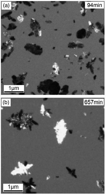
  • Fig. 1 shows TEM images of partially crystallized HWCVD and PECVD a-Si:H films annealed at 600 °C, with the annealing times indicated in the figures.
  • From this figure, clear differences are seen not only in the anneal time, but also in the grain density and grain morphology between the different films.
  • These differences become even more pronounced when a low CH HWCVD film is included in the comparison compared to the PECVD film seen in Fig. 1(b) [8,9]; in these comparisons, the PECVD film showed much lower grain densities and larger grains overall.
  • In Table 3 the authors first present a review of the NMR data, from which the densities of the isolated and clustered hydrogen distributions can be obtained.
  • H calculation, the authors use an averaged value of the clustered/isolated hydrogen ratio, obtained for ‘standard’ (low deposition rate) films deposited using 100% silane and a moderate (∼ 200–250 C) substrate temperature, also known as For the PECVD a-Si.

4. Summary and conclusions

  • The authors have presented the crystallization kinetics when HWCVD films of different film CH and ‘standard’ PECVD aSi:H films have been annealed at a temperature of 600 °C to induce film crystallization.
  • The authors find that the low CH HWCVD film nucleates first, and that the incubation time increases with increasing film CH.
  • Not surprisingly, the films which nucleate the fastest contain the smallest grains when crystallization is complete.
  • The increase in short range disorder upon film hydrogen evolution does not seem to play a primary role in the crystallization process.
  • A tentative model relating the crystallization kinetics to the initial hydrogen spatial distribution in the film is presented.

Did you find this useful? Give us your feedback

Citations
More filters
Journal ArticleDOI
TL;DR: In this article, it was shown that nucleation in thermally annealed hydrogenated amorphous silicon occurs in the more well ordered spatial regions in the network, which are defined by the initial inhomogeneous H distributions in the as-grown films.
Abstract: Utilizing the concepts of a critical crystallite size and local film inhomogeneity, it is shown that nucleation in thermally annealed hydrogenated amorphous silicon occurs in the more well ordered spatial regions in the network, which are defined by the initial inhomogeneous H distributions in the as-grown films. Although the film H evolves very early during annealing, the local film order is largely retained in the still amorphous films even after the vast majority of the H is evolved, and the more well ordered regions which are the nucleation center sites for crystallization are those spatial regions which do not initially contain clustered H, as probed by H NMR spectroscopy. The sizes of these better ordered regions relative to a critical crystallite size determine the film incubation times (the time before the onset of crystallization). Changes in film short range order upon H evolution, and the presence of microvoid type structures in the as grown films play no role in the crystallization process. While the creation of dangling bonds upon H evolution may play a role in the actual phase transformation itself, the film defect densities measured just prior to the onset of crystallization exhibit no trends which can be correlated with the film incubation times.

23 citations

Journal ArticleDOI
TL;DR: In this paper, the effect of the microstructure of remote plasma-deposited amorphous silicon films on the grain size development in polycrystalline silicon upon solid-phase crystallization is reported.
Abstract: In this paper the effect of the microstructure of remote plasma-deposited amorphous silicon films on the grain size development in polycrystalline silicon upon solid-phase crystallization is reported. The hydrogenated amorphous silicon films are deposited at different microstructure parameter values R* (which represents the distribution of SiHx bonds in amorphous silicon), at constant hydrogen content. Amorphous silicon films undergo a phase transformation during solid-phase crystallization and the process results in fully (poly-)crystallized films. An increase in amorphous film structural disorder (i.e., an increase in R*), leads to the development of larger grain sizes (in the range of 700-1100 nm). When the microstructure parameter is reduced, the grain size ranges between 100 and 450 nm. These results point to the microstructure parameter having a key role in controlling the grain size of the polycrystalline silicon films and thus the performance of polycrystalline silicon solar cells.

23 citations

Journal ArticleDOI
TL;DR: Amorphous Si (a-Si) films with lower hydrogen contents show better adhesion to glass during flash lamp annealing (FLA), whereas a-Si films deposited by catalytic CVD (Cat-CVD) partially adhere even after crystallization as mentioned in this paper.

21 citations

Journal ArticleDOI
15 Jun 2021
TL;DR: In this article, the growth conditions of nc-Si:H thin films as the carrier-selective layers for SHJ solar cells are reviewed and the surface and growth zone models are analyzed at different stages of incubation, nucleation and growth of the silicon nanocrystallites within the hydrogenated amorphous silicon matrix.
Abstract: Doped nanocrystalline silicon (nc-Si:H) thin films offer improved carrier transport characteristics and reduced parasitic absorption compared to amorphous silicon (a-Si:H) films for silicon heterojunction (SHJ) solar cell application. In this article, we review the growth conditions of nc-Si:H thin films as the carrier-selective layers for SHJ solar cells. Surface and growth zone models are analysed at different stages of incubation, nucleation, and growth of the silicon nanocrystallites within the hydrogenated amorphous silicon matrix. The recent developments in the implementation of nc-Si:H films and oxygen-alloyed nc-SiOx:H films for SHJ cells are highlighted. Furthermore, hydrogen and carbon dioxide plasma treatments are emphasised as the critical process modification steps for augmenting the nc-Si:H films' optoelectronic properties to enhance the SHJ device performance with better carrier-selective interfaces.

19 citations

Journal ArticleDOI
TL;DR: In this article, an analytical solution for the crystallization kinetics in the special case of plate-shaped samples with a finite thickness is presented. But the analytical solution does not reveal the thickness range which influences the isothermal crystallization mode significantly.
Abstract: The Johnson–Mehl–Avrami–Kolmogorov (JMAK) model is widely used to quantify the isothermal crystallization kinetics. The present work reports an analytical solution for the crystallization kinetics in the special case of plate-shaped samples with a finite thickness. As a result, we obtained an adapted JMAK model revealing the thickness range which influences the crystallization kinetics mode significantly. The analytical solution also provides theoretical bounds for the film thickness, where the assumption of 2D or 3D kinetics is accurate. Finally, the conclusions related to amorphous silicon and amorphous nickel-titanium thin films are reported.

17 citations

References
More filters
Journal ArticleDOI
TL;DR: In this paper, it was shown that hydrogenated amorphous silicon containing as little as 1/10 the bonded H observed in device-quality glow discharge films have been deposited by thermal decomposition of silane on a heated filament.
Abstract: Device‐quality hydrogenated amorphous silicon containing as little as 1/10 the bonded H observed in device‐quality glow discharge films have been deposited by thermal decomposition of silane on a heated filament. These low H content films show an Urbach edge width of 50 mV and a spin density of ∼1/100 as large as that of glow discharge films containing comparable amounts of H. High substrate temperatures, deposition in a high flux of atomic H, and lack of energetic particle bombardment are suggested as reasons for this behavior.

464 citations

Journal ArticleDOI
TL;DR: It is shown that the width of the ``optic peak'' increases roughly linearly with the rms bond-angle distortion of the network, consistent with model-building experience which shows that it is impossible to construct fully bonded amorphous networks with \ensuremath{\Delta}${\ensureMath{\theta}}_{b}$.
Abstract: The Raman scattering from various model structures for amorphous silicon is computed. It is shown that the width of the ``optic peak'' increases roughly linearly with the rms bond-angle distortion \ensuremath{\Delta}${\ensuremath{\theta}}_{b}$ of the network. The experimentally observed linewidths lead to 7.7\ifmmode^\circ\else\textdegree\fi{}\ensuremath{\le}\ensuremath{\Delta}${\ensuremath{\theta}}_{b}$\ensuremath{\le}10.5\ifmmode^\circ\else\textdegree\fi{}. The smaller linewidths (and hence angles) correspond to networks that have been annealed at higher temperatures. These results are consistent with model-building experience which shows that it is impossible to construct fully bonded amorphous networks with \ensuremath{\Delta}${\ensuremath{\theta}}_{b}$\ensuremath{\le}6.6\ifmmode^\circ\else\textdegree\fi{}.

392 citations

Journal ArticleDOI
TL;DR: In this paper, the morphological evolution of the amorphous towards the polycrystalline phase is investigated by transmission electron microscopy and it is interpreted in terms of a physical model containing few free parameters related to the thermodynamical properties of ammorphous silicon and to the kinetical mechanisms of crystal grain growth.
Abstract: The solid phase crystallization of chemical vapor deposited amorphous silicon films onto oxidized silicon wafers, induced either by thermal annealing or by ion beam irradiation at high substrate temperatures, has been extensively developed and it is reviewed here. We report and discuss a large variety of processing conditions. The structural and thermodynamical properties of the starting phase are emphasized. The morphological evolution of the amorphous towards the polycrystalline phase is investigated by transmission electron microscopy and it is interpreted in terms of a physical model containing few free parameters related to the thermodynamical properties of amorphous silicon and to the kinetical mechanisms of crystal grain growth. A direct extension of this model explains also the data concerning the ion-assisted crystal grain nucleation.

332 citations

Journal ArticleDOI
TL;DR: In this paper, a theoretical and experimental study of the recrystallization behavior of polycrystalline silicon films amorphized by self-implantation was carried out and the crystallization behavior was found to be similar to the crystallisation behavior of films deposited in the amorphous state, however, a transient time was observed, during which negligible crystallization occurs.
Abstract: This paper presents a theoretical and experimental study of the recrystallization behavior of polycrystalline silicon films amorphized by self‐implantation. The crystallization behavior was found to be similar to the crystallization behavior of films deposited in the amorphous state, as reported in the literature; however, a transient time was observed, during which negligible crystallization occurs. The films were prepared by low‐pressure chemical vapor deposition onto thermally oxidized silicon wafers and amorphized by implantation of silicon ions. The transient time, nucleation rate, and characteristic crystallization time were determined from the crystalline fraction and density of grains in partially recrystallized samples for anneal temperatures from 580 to 640 °C. The growth velocity was calculated from the nucleation rate and crystallization time and is lower than values in the literature for films deposited in the amorphous state. The final grain size, as calculated from the crystallization param...

329 citations

Journal ArticleDOI
TL;DR: Using the fact that multiple-quantum excitation is limited by the size of the dipolar-coupled spin system, it is shown that the predominant bonding environment for hydrogen is a cluster of four to seven atoms.
Abstract: Multiple-quantum nuclear-magnetic-resonance techniques are used to study the distribution of hydrogen in hydrogenated amorphous silicon. Using the fact that multiple-quantum excitation is limited by the size of the dipolar-coupled spin system, we show that the predominant bonding environment for hydrogen is a cluster of four to seven atoms. For device quality films, the concentration of these cluster defects increases with increasing hydrogen content. At very high hydrogen content, the clusters are replaced with a continuous network of silicon-hydrogen bonds.

174 citations

Frequently Asked Questions (1)
Q1. What contributions have the authors mentioned in the paper "A comparison of grain nucleation and grain growth during crystallization of hwcvd and pecvd a-si:h films" ?

Even though the bonded hydrogen evolves very early from the film during annealing, the authors suggest that the initial spatial distribution of hydrogen plays a critical role in the crystallization kinetics, and they propose a preliminary model to describe this process.