scispace - formally typeset
Search or ask a question
Journal ArticleDOI

A comprehensive model of PMOS NBTI degradation

01 Jan 2005-Microelectronics Reliability (Pergamon)-Vol. 45, Iss: 1, pp 71-81
TL;DR: A comprehensive model for NBTI phenomena within the framework of the standard reaction–diffusion model is constructed and it is demonstrated how to solve the reaction-diffusion equations in a way that emphasizes the physical aspects of the degradation process and allows easy generalization of the existing work.
About: This article is published in Microelectronics Reliability.The article was published on 2005-01-01 and is currently open access. It has received 710 citations till now. The article focuses on the topics: Negative-bias temperature instability.

Summary (5 min read)

1.1. Background

  • The instability of PMOS transistor parameters (e.g., threshold voltage, transconductance, saturation current, etc.) under negative bias and relatively high temperature has been known to be a reliability concern since the 1970s [1–4], and modeling effort to understand this is also just as old [5].
  • (a) Introduction of CMOS in early 1980s that has made PMOS and NMOS devices equally important for IC designs, also known as These changes include.
  • Since hydrogen diffusion through poly-silicon is faster than that in oxide, scaling of gate oxides has increased NBTI susceptibilities [16].
  • These technological factors, along with other circuit specific usages, have made NBTI as one of the foremost reliability concerns for modern integrated circuits (almost as important as of gate oxide TDDB reliability).

1.2. Experimental signatures of NBTI

  • Any theory of NBTI must be able to explain the following observations regarding the NBTI phenomena [7–27].
  • There are intriguing deviations from the perfect, single-exponent power-law degradation that needs careful analysis.
  • The authors will use the above experimental observations to systematically test the R–D model whenever possible and augment the model whenever necessary.

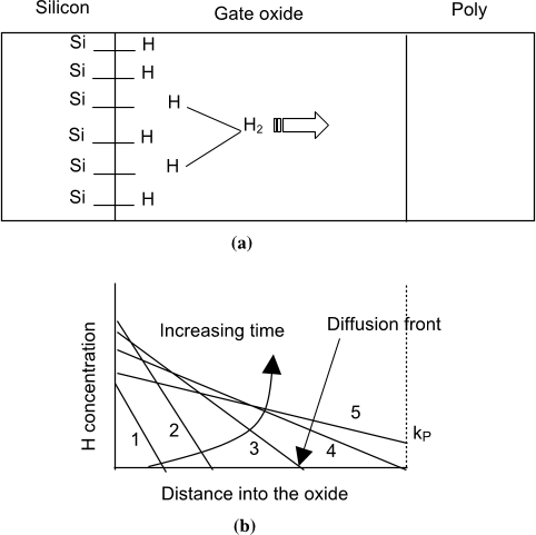
2.1. Description of the R–D model

  • Till date, the R–D model is the only model that can interpret the power-law dependence of interface trap generation during NBTI, as discussed in Section 1.2(a), without making any a priori assumption regarding the distribution of interface bond-strengths.
  • Note that no field dependent term in Eq. (1c) means that the diffusing species is assumed neutral.
  • S) and H. Initial interface-trap generation rate depends on Si–H val .
  • This would lead to a sharper gradient interface, and would trigger enhanced interface trap generation.
  • First, one can theoretically estimate the bulk-trap contribution for a given oxide thickness for every stress voltage and temperature [15,28] and subtract this contribution to extract the NIT contribution from measured DVT data.

2.2.1. Stress phase

  • Also, x ¼ ðDHtÞ1=2 from Eq. (1c) implies that the hydrogen diffusion front is yet to reach the poly-silicon interface.
  • This regime (n ¼ 1=2) is likely to be observed in thinner oxides where the diffusion front would reach the poly-interface within measurement window.

2.2.2. Annealing phase

  • Apart from the five-phase degradation discussed above, another key prediction of the R–D model is similar multi-phase annealing of the interface traps (created during the stress phase) once the stress is removed (see Section 1.2(b)).
  • Once the stress is removed, the dissociation of the Si–H bond that forced forward diffusion of hydrogen away from the interface no longer exists, therefore the hydrogen can now diffuse back and recombine with silicon dangling bonds restoring them to their passive Si–H state.
  • This diffusion controlled annealing phase (analogous to the diffusion-controlled generation phase described by Eq. (2a)) can be treated analytically in the following manner [20].
  • Fig. 4 shows that Eqs. (2a) and (2c) can interpret the stress and the relaxation phases of the NBTI degradation well.
  • This is yet another indication that the diffusing species is charge neutral, because a positively charged species would diffuse asymmetrically with stress bias and anneal (zero) bias conditions, which would have made Eq. (2c) inconsistent with experimental data.

2.3. Discussion of the R–D model

  • The R–D model successfully explains both the powerlaw dependence of interface trap generation and the mechanics of interface trap annealing––the two key features of NBTI as discussed in Section 1.2(a) and (b).
  • It does so without requiring that holes be present for NBTI degradation (although it does not forbid it either) and apart from requiring that the diffusing species be neutral, the theory places no restriction on the nature or type of diffusing species involved.
  • Furthermore, it offers no quantitative predictions regarding the field or temperature dependence of the NBTI phenomena.
  • Therefore, one cannot optimize operating or processing conditions to reduce NBTI effects using the basic R–D model.
  • Moreover, the predictions of precise power-exponents (e.g., n ¼ 1=4) also make the R–D model difficult to reconcile with wide variety of exponents observed in various experiments.

3.1. Model for NBTI field (or voltage) dependence

  • According to the R–D model, the field dependence of the NBTI phenomena must be confined to the processes at the interface (kF and kR) because the diffusing species is charge neutral.
  • The authors anticipate that the forward dissociation constant, kF, should depend on the number of holes (p), their ability to tunnel to the Si–H bonds , the capture cross-section of the Si–H bonds (r0), and any field dependence of Si–H bond dissociation (B), so that kFð. . .
  • The authors discuss these individual processes below.

3.1.1. Role of holes and field-dependence through hole density

  • The presence of holes have been linked to NBTI degradation from the beginning of the study of this process––in part because the effect was first observed in PMOS devices in inversion.
  • The lack of degradation in NMOS devices stressed in accumulation with voltages similar to those used for PMOS NBTI tests have sometimes been used to argue against the role of holes in NBTI degradation [12].
  • Since the authors must compare the NBTI degradation at comparable hole densities, the surface field must be same––which means that the NMOS must be stressed approximately one volt higher compared to PMOS devices for comparable NBTI effects (to take care of flatband voltage difference).
  • Fig. 5 shows that this is indeed the case––this explains the experimental observation discussed in Section 1.2(c) and leads us to conclude that the presence of holes play a key role in NBTI degradation consistent with the observation in Section 1.2(c).

3.1.2. Role of hole capture and its field-dependence

  • Once the holes are available, they must tunnel through the interface layer of 1–2 A to be captured by the Si–H bonds.
  • The field dependent tunneling coefficient depends exponentially on the local electric field at the interface (e.g., TCOEFF expðEOX=E0), although other forms are also suitable [1,2,15,23]).
  • Fig. 6 shows that this is indeed the case for oxides of various thicknesses, confirming the general validity of the approach [24–26,28].

3.1.3. Role of field-dependent bond-dissociation

  • A key unknown is the influence of the electric field on the dissociation of the Si–H bond itself.
  • Assuming that such modification will be associated with a reduction in the barrier height of the bond dissociation, the authors anticipate that there may be field dependent activation energy associated with this process.

3.1.4. Role of bulk traps

  • Finally, as discussed earlier in the paper, it is important to realize that at high negative electric fields (especially for thicker gate oxides that involve large stress voltages) NBTI data are often contaminated by generation of bulk traps [15].
  • Such contribution from bulk traps must be isolated before a universal representation of kF (Eq. (3a)) can be found.
  • According to the Anode Hole Injection model, at large negative voltages in both PMOS and NMOS transistors, electrons are injected from the poly-gate into the silicon substrate.
  • These energetic electrons in turn produce hot holes that are injected back into the oxide-creating bulk defects within the oxides [28].
  • Once such corrections are accounted for, the authors find that field dependence of Eq. (3a) defines the forward reaction rate well and is consistent with the observation in Section 1.2.

3.2.1. Concept of universal scaling

  • Eq. (2a) provides a universal scaling relationship that can used to decouple the field- and temperature-depen- dence of NBTI.
  • This equation predicts that if the stress time is measured in units of (1=DH) and if the trap density is normalized by ðkFN0=kRÞ1=2, then the resulting curve should be universal.
  • Moreover, since DH is a function of temperature alone and is independent of electric field, and since ðkFN0=kRÞ1=2 is field dependent, but temperature independent (approximately, see below), the NBTI curves at different temperatures (but at a constant electric field) can be scaled along the time axis to identify the activation energy of the diffusion process [14–16].
  • Fig. 8 highlights the scaling methodology and shows that universal scaling holds for NBTI data measured under a wide range of stress bias and temperature.

3.2.2. Activation energy of the diffusion process

  • The dissociation and annealing of Si–H bonds (kF and kR) and the diffusion of hydrogen (DH) through the oxide are not.
  • The authors use two methods to determine the activation energies.
  • The first method uses the time–scaling idea discussed above that allows us to determine Ea directly (Fig. 8).
  • Therefore, the temperature activation of NBTI process is essentially determined by that of the diffusion process, i.e., EaðNBTIÞ EaðDHÞ=4¼ 0:12–0:15 eV-consistent with Section 1.2(e).

3.2.3. Debate regarding the nature of the diffusing species

  • H, and H2O have been suggested), the activation energy of the diffusing species (EaðDHÞ ¼ 4EaðNBTIÞ 0:5 eV) appears to indicate that the diffusing species is hydrogen, most probably a molecular species [32].
  • Moreover, the experiment in Ref. [10], when viewed in light of Eq. (2a), also supports the hydrogen hypothesis:.
  • When hydrogen annealing of Si-dangling bonds to create Si–H bonds is replaced with deuterium annealing to create Si–D bonds, Eq. (2a) anticipates that NITðDÞ=NITðHÞ ¼ ðDD=DHÞ1=4 ¼ ðmD=mHÞ1=8 (mH and mD being the effective mass of hydrogen and deuterium respectively), making the dependence finite but weak [10].
  • Note that if –OH were the diffusing species, the difference in masses of –OH and –OD would have been small, resulting in essentially indistinguishable impact of deuterium annealing.
  • The lack of strong deuterium effect also highlights the chemical nature of the Si–H (or Si–D) bond breaking as opposed to the kinetic nature of Si–H bond breaking during HCI experiments.

3.2.4. Hypothesis regarding the non-standard NBTI exponents

  • The R–D model predicts very precise power-law exponent that is independent of temperature, time, or oxide thickness (e.g., n ¼ 1=4 analytically, or n ¼ 0:25–0:28 numerically).
  • Since the assumption of constant diffusion coefficient is only appropriate for isotropic media with spatially and temporally uniform hopping rates, this may not be appropriate for diffusion in amorphous media where the hopping distances and hopping times are exponentially distributed [33–35].
  • Therefore, at lower-temperature, the observed power-exponents are typically lower, as shown in Fig. 10.
  • In time however a fraction of hydrogen will eventually find themselves trapped in deeper levels with long release time, making the asymptotic n0 value similar to that of the low-temperature value [15].
  • The hypothesis discussed above, if supported by other experiments, would imply that more amorphous the oxide, the better is its NBTI performance, because deep level trapping with long release time would reduce NBTI power-exponent.

4. Conclusions

  • The authors have discussed a theory of NBTI that uses the theoretical framework of R–D model to encapsulate the field, temperature, and processing dependencies of the NBTI phenomena.
  • This overall framework allows one to discuss and optimize the operating and processing conditions in a manner that is globally consistent and technologically relevant.
  • The model presented here still lacks systematic description of the role of boron and nitrogen at the interface.
  • Such processing details will surely affect the magnitudes of both kF and kR (but most probably will not modify the functional dependence on field and temperature as discussed in this paper).

Did you find this useful? Give us your feedback

Figures (10)
Citations
More filters
Proceedings ArticleDOI
24 Jul 2006
TL;DR: A predictive model is developed for the degradation of NBTI in both static and dynamic operations and key insights are obtained for the development of robust design solutions.
Abstract: Negative bias temperature instability (NBTI) has become the dominant reliability concern for nanoscale PMOS transistors. In this paper, a predictive model is developed for the degradation of NBTI in both static and dynamic operations. Model scalability and generality are comprehensively verified with experimental data over a wide range of process and bias conditions. By implementing the new model into SPICE for an industrial 90nm technology, key insights are obtained for the development of robust design solutions: (1) the most effective techniques to mitigate the NBTI degradation are V/sub DD/ tuning, PMOS sizing, and reducing the duty cycle; (2) an optimal V/sub DD/ exists to minimize the degradation of circuit performance; (3) tuning gate length or the switching frequency has little impact on the NBTI effect; (4) a new switching scenario is identified for worst case timing analysis during NBTI stress.

460 citations

Proceedings ArticleDOI
01 Sep 2006
TL;DR: This paper presents a predictive model for the negative bias temperature instability (NBTI) of PMOS under both short term and long term operation based on the reaction-diffusion (R-D) mechanism, which accurately captures the dependence of NBTI on the oxide thickness, the diffusing species and other key transistor and design parameters.
Abstract: This paper presents a predictive model for the negative bias temperature instability (NBTI) of PMOS under both short term and long term operation. Based on the reaction-diffusion (R-D) mechanism, this model accurately captures the dependence of NBTI on the oxide thickness (tox), the diffusing species (H or H2) and other key transistor and design parameters. In addition, a closed form expression was derived for the threshold voltage change (DeltaVth ) under multiple cycle dynamic operation. Model accuracy and efficiency were verified with 90-nm experimental and simulation data. The impact of NBTI was further investigated on representative digital circuits

431 citations


Cites background from "A comprehensive model of PMOS NBTI ..."

  • ...Firstly, oxide thickness was assumed to be infinite and the polysilicon was considered either as a reflector or absorber [1]....

    [...]

Journal ArticleDOI
James H. Stathis1, Sufi Zafar1
TL;DR: Negative bias temperature instability (NBTI) as discussed by the authors is a critical reliability phenomenon in advanced CMOS technology, in which interface traps and positive oxide charge are generated in metaloxide-silicon (MOS) structures under negative gate bias, in particular at elevated temperature.

373 citations

01 Jan 2006
TL;DR: This review includes comprehensive summaries of the basic phenomenology, including time- and frequency-dependent effects (relaxation), and process dependences; theory, including drift–diffusion models and microscopic models for interface states and fixed charge, and the role of nitrogen; and the practical implications for circuit performance and new gate-stack materials.
Abstract: Negative bias temperature instability (NBTI), in which interface traps and positive oxide charge are generated in metal–oxide–silicon (MOS) structures under negative gate bias, in particular at elevated temperature, has come to the forefront of critical reliability phenomena in advanced CMOS technology. The purpose of this review is to bring together much of the latest experimental information and recent developments in theoretical understanding of NBTI. The review includes comprehensive summaries of the basic phenomenology, including time- and frequency-dependent effects (relaxation), and process dependences; theory, including drift–diffusion models and microscopic models for interface states and fixed charge, and the role of nitrogen; and the practical implications for circuit performance and new gate-stack materials. Some open questions are highlighted. � 2005 Elsevier Ltd. All rights reserved.

348 citations


Cites background or methods from "A comprehensive model of PMOS NBTI ..."

  • ...Numerical simulations have given values that are both somewhat larger [61] and smaller [63]....

    [...]

  • ...Another useful relation sometimes invoked in treatments of NBTI is the conservation rule [29,61,62]...

    [...]

  • ...According to some viewpoints, therefore, bulk positive charge generation is a separate process involving trapping of holes, not defect generation via a low-field reaction [61,65,79]....

    [...]

  • ...Another description of the effect of oxide thickness has claimed that the time dependence changes to t when the diffusion front of X reaches the gate electrode [61]....

    [...]

  • ...[50,63] Si–H + h M Si + H [61,63] Si–H þ hþ $ Si þ þ 2H2 [63] Si–H + hMSi +H [63,78] Si–H + H M Si + + H2...

    [...]

Journal ArticleDOI
TL;DR: The general conclusion is that although much is understood about NBTI, several aspects are poorly understood.

347 citations


Cites background from "A comprehensive model of PMOS NBTI ..."

  • ..., the gate voltages on n- and p-channel devices are not the same for a given oxide electric field [5]....

    [...]

  • ...In this paper, I will draw upon the excellent recent reviews by Stathis and Zafar [3], Huard et al. [4], and Alam and Mahapatra [5] as well as many other papers published in the last few years....

    [...]

  • ...[4], and Alam and Mahapatra [5] as well as many other papers published in the last few years....

    [...]

References
More filters
Journal ArticleDOI
TL;DR: In this paper, the authors developed a stochastic transport model for the transient photocurrent, which describes the dynamics of a carrier packet executing a time-dependent random walk in the presence of a field-dependent spatial bias and an absorbing barrier at the sample surface.
Abstract: Measurements of the transient photocurrent $I(t)$ in an increasing number of inorganic and organic amorphous materials display anomalous transport properties. The long tail of $I(t)$ indicates a dispersion of carrier transit times. However, the shape invariance of $I(t)$ to electric field and sample thickness (designated as universality for the classes of materials here considered) is incompatible with traditional concepts of statistical spreading, i.e., a Gaussian carrier packet. We have developed a stochastic transport model for $I(t)$ which describes the dynamics of a carrier packet executing a time-dependent random walk in the presence of a field-dependent spatial bias and an absorbing barrier at the sample surface. The time dependence of the random walk is governed by hopping time distribution $\ensuremath{\Psi}(t)$. A packet, generated with a $\ensuremath{\Psi}(t)$ characteristic of hopping in a disordered system [e.g., $\ensuremath{\Psi}(t)\ensuremath{\sim}{t}^{\ensuremath{-}(1+\ensuremath{\alpha})}$, $0l\ensuremath{\alpha}l1$], is shown to propagate with a number of anomalous non-Gaussian properties. The calculated $I(t)$ associated with this packet not only obeys the property of universality but can account quantitatively for a large variety of experiments. The new method of data analysis advanced by the theory allows one to directly extract the transit time even for a featureless current trace. In particular, we shall analyze both an inorganic ($a\ensuremath{-}{\mathrm{As}}_{2}{\mathrm{Se}}_{3}$) and an organic (trinitrofluorenone-polyvinylcarbazole) system. Our function $\ensuremath{\Psi}(t)$ is related to a first-principles calculation. It is to be emphasized that these $\ensuremath{\Psi}(t)$'s characterize a realization of a non-Markoffian transport process. Moreover, the theory shows the limitations of the concept of a mobility in this dispersive type of transport.

2,610 citations

Book
01 Jan 1983
TL;DR: The formation of amorphous solids Amorphous Morphology: The Geometry and Topology of Disorder Chalcogenide Glasses and Organic Polymers The Percolation Model Localization Delocalization Transitions Optical and Electrical Properties Index as discussed by the authors.
Abstract: The Formation of Amorphous Solids Amorphous Morphology: The Geometry and Topology of Disorder Chalcogenide Glasses and Organic Polymers The Percolation Model Localization Delocalization Transitions Optical and Electrical Properties Index.

2,051 citations

Journal ArticleDOI
TL;DR: The negative bias temperature instability (NBTI) commonly observed in p-channel metaloxide-semiconductor field effect transistors when stressed with negative gate voltages at elevated temperatures is discussed in this article.
Abstract: We present an overview of negative bias temperature instability (NBTI) commonly observed in p-channel metal–oxide–semiconductor field-effect transistors when stressed with negative gate voltages at elevated temperatures. We discuss the results of such stress on device and circuit performance and review interface traps and oxide charges, their origin, present understanding, and changes due to NBTI. Next we discuss the effects of varying parameters (hydrogen, deuterium, nitrogen, nitride, water, fluorine, boron, gate material, holes, temperature, electric field, and gate length) on NBTI. We conclude with the present understanding of NBTI and its minimization.

1,033 citations


Additional excerpts

  • ...2004 Published by Elsevier Ltd....

    [...]

Journal ArticleDOI
TL;DR: A detailed study of the increase of the number of surface traps in MOS structures after NBS at temperatures (25-125°C) and fields (400-700 MV/m) comparable to those used in MNOS devices is presented in this article.
Abstract: One of the most important degradation effects observed in MNOS memory transistors is a negative shift of the threshold window. This negative shift is caused by a strong increase of the density of Si‐SiO2 surface traps. This effect has been proposed to be caused by the same effect that is observed in MOS devices subjected to negative‐bias stress (NBS). In this paper, a detailed study of the increase of the number of surface traps in MOS structures after NBS at temperatures (25–125 °C) and fields (400–700 MV/m) comparable to those used in MNOS devices is presented. Two different behaviors are observed. At low fields the surface‐trap density increases as t1/4 and at high fields it increases linearly with the stress time t. The low‐field behavior is temperature and field dependent and the zero‐field activation energy is determined to be 0.3 eV. The high‐field behavior is strongly field dependent but independent of temperature. A physical model is proposed to explain the surface‐trap growth as being diffusion ...

678 citations


"A comprehensive model of PMOS NBTI ..." refers methods in this paper

  • ...In this paper, we construct a comprehensive model for NBTI phenomena within the framework of the standard reaction–diffusion model....

    [...]

Journal ArticleDOI
TL;DR: In this paper, the surface state charge associated with thermally oxidized silicon has been studied experimentally using MOS structures and the results indicate that the surface-state charge can be reproducibly controlled over a range 1010-1012 cm -2, and it is an intrinsic property of the silicon dioxide-silicon system.
Abstract: The nature of the surface-state charge (Qss) associated with thermally oxidized silicon has been studied experimentally using MOS structures. The effects of oxidation conditions, silicon orientation, annealing treatments, oxide thickness, and electric field were examined, as well as the physical location of the surface-state charge. The results indicate that the surface-state charge can be reproducibly controlled over a range 1010-1012 cm -2, and that it is an intrinsic property of the silicon dioxide-silicon system. It appears to be due to an excess silicon species introduced into the oxide layer near the silicon during the oxidation process.

673 citations


"A comprehensive model of PMOS NBTI ..." refers methods in this paper

  • ...In this paper, we construct a comprehensive model for NBTI phenomena within the framework of the standard reaction–diffusion model....

    [...]

Frequently Asked Questions (2)
Q1. What contributions have the authors mentioned in the paper "A comprehensive model of pmos nbti degradation" ?

In this paper, the authors construct a comprehensive model for NBTI phenomena within the framework of the standard reaction–diffusion model. The authors demonstrate how to solve the reaction–diffusion equations in a way that emphasizes the physical aspects of the degradation process and allows easy generalization of the existing work. The authors also augment this basic reaction–diffusion model by including the temperature and field-dependence of the NBTI phenomena so that reliability projections can be made under arbitrary circuit operating conditions. 

One of the key goal of their future work would be to clarify the role of such processing changes on NBTI performance.