scispace - formally typeset
Search or ask a question
Journal ArticleDOI

A High-IIP3 Third-Order Elliptic Filter With Current-Efficient Feedforward-Compensated Opamps

TL;DR: A low-distortion active filter is realized using current-efficient feedforward-compensated operational amplifiers in the integrators and feedforward current injection in the summing amplifier to counter process variations and set the bandwidth accurately.
Abstract: A low-distortion active filter is realized using current-efficient feedforward-compensated operational amplifiers in the integrators and feedforward current injection in the summing amplifier. A third-order elliptic low-pass filter with two possible bandwidth settings of 17 and 8.5 MHz consumes 1.8 mW from a 1.8-V supply and occupies 0.17 mm2 in a 0.18- μm CMOS process. The measured maximum signal-to-noise and distortion ratios at the two bandwidth settings are 50.5 and 52.5 dB, respectively. The corresponding third-order intermodulation intercept points (IIP3) are +28.2 and +30.8 dBm. Automatic tuning is used at the startup to counter process variations and set the bandwidth accurately.

Summary (2 min read)

Introduction

  • A switchable bandwidth is required for multistandard radios.
  • Among integrated continuous-time filters, active RC filters provide the best distortion performance at medium frequencies because they consist of integrators and amplifiers using operational amplifiers in negative feedback loops, which suppress the distortion arising from active elements.
  • The output current driven from the opamp can be reduced by injecting a replica of the current to the output through a separate path [6].

II. THIRD-ORDER ELLIPTIC FILTER

  • Fig. 1(a) shows the block diagram of the third-order elliptic filter.
  • The integrator outputs are scaled for equal maximum transfer function magnitude.
  • A 5-bit control word b〈4 : 0〉 switches the resistors and the capacitors and varies the RC product from 55% to 175% of the midcode value to compensate for process variations.
  • The automatic tuning scheme is shown in Fig. 1(c).
  • After five cycles of successive approximation, the bits converge to a value that sets the time constant of the replica integrator to 100 ns.

III. ADVANTAGES OF FEEDFORWARD OPAMPS

  • Fig. 2 shows the macromodels of the feedforward- and Miller-compensated opamps.
  • The first stage consists of gm1 loaded by RL1 and C1, and the second stage consists of gm2 loaded by RL2 and CL.
  • The distortion of the filter with feedforward-compensated opamps is significantly lower than that with Miller-compensated opamps.
  • The input-referred noise voltage of the two opamps is the same because the same value of gm1 is used for both.

IV. CURRENT-EFFICIENT FEEDFORWARD OPAMP

  • Fig. 4 shows the feedforward-compensated opamp proposed in [5].
  • Feedforward compensation is provided by using another nMOS differential pair M3.
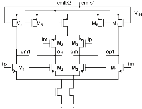
  • Separate common-mode feedback circuit (CMFB) stages are used to drive current sources M4 and M5 and to stabilize the common-mode output of each stage.
  • The common-mode voltage is fed back through gm,cm (a differential pair with a current mirror load).
  • The opamp consumes about 0.2 mA and is used for all integrators and the summing amplifier in Fig. 1.

V. SUMMING AMPLIFIER

  • Fig. 7(a) shows the conventional summing amplifier.
  • Because multiple inputs are summed, the loop gain tends to be lower, and the distortion tends to be higher than in an amplifier with a single input.
  • With a real opamp, the virtual ground experiences a signal swing proportional to (a1x1 + a2x2 + a3x3)/R, i.e., the current driven from the opamp.
  • Conventionally, this is done by increasing the gain of the opamp (at the relevant signal frequencies).
  • In their implementation [see Fig. 7(c)], only a3x3/R, which is the largest component of the output current, is injected to the output using a transconductor.

VI. MEASURED RESULTS

  • The third-order filter with automatic tuning is fabricated in a 0.18-μm CMOS process.
  • Fig. 8 shows the layout, the test schematic, and the test board.
  • In the small number of characterized samples, the 3-dB bandwidth after automatic tuning is 16.3–16.6 MHz in the high-bandwidth mode and 7.5–8.4.
  • As expected, the worst cases occur near the band edges due to peaking in the magnitude response at the internal nodes.
  • The worst case inband IIP3 values at the high- and low-bandwidth settings are +28.2 and +30.8 dBm, respectively.

VII. CONCLUSION

  • Power-efficient feedforward-compensated opamps in the integrators and feedforward current injection in the summing amplifier enable filters with an inherently high IIP3.
  • The power dissipation depends on the signal level.
  • The FOM of the filters presented here is better than those that have a comparably narrow transition band.
  • 1At an input signal level equal to the IIP3, the IM3 (extrapolated from smallsignal levels) is also equal to the IIP3.
  • 2Where the integrated noise is not reported, it is calculated by multiplying the inband spectral density by the square root of the bandwidth.

Did you find this useful? Give us your feedback

Content maybe subject to copyright    Report

IEEE TRANSACTIONS ON CIRCUITS AND SYSTEMS—II: EXPRESS BRIEFS, VOL. 58, NO. 4, APRIL 2011 205
A High-IIP3 Third-Order Elliptic Filter With
Current-Efficient Feedforward-Compensated Opamps
Nagendra Krishnapura, Abhishek Agrawal, and Sameer Singh
Abstract—A low-distortion active filter is realized using current-
efficient feedforward-compensated operational amplifiers in the
integrators and feedforward current injection in the summing
amplifier. A third-order elliptic low-pass filter with two possible
bandwidth settings of 17 and 8.5 MHz consumes 1.8 mW from a
1.8-V supply and occupies 0.17 mm
2
in a 0.18-μm CMOS process.
The measured maximum signal-to-noise and distortion ratios at
the two bandwidth settings are 50.5 and 52.5 dB, respectively. The
corresponding third-order intermodulation intercept points (IIP3)
are +28.2 and +30.8 dBm. Automatic tuning is used at the startup
to counter process variations and set the bandwidth accurately.
Index Terms—Automatic tuning, continuous-time filters, elliptic
filters, feedforward compensation.
I. INTRODUCTION
I
N zero-intermediate-frequency integrated-circuit radio re-
ceivers, low-pass filters [1]–[3] are used before analog/
digital conversion. Their bandwidths range from a few mega-
hertz to a few tens of megahertz. A switchable bandwidth is re-
quired for multistandard radios. For example, 802.11 [wireless
local-area network (WLAN)] has twice the signal bandwidth
in the “n” mode as in the “a, b, and g” modes [4]. Another
important requirement for these filters is a low distortion per-
formance, usually specified using the third-order intermodula-
tion intercept point (IIP3). Among integrated continuous-time
filters, active RC filters provide the best distortion performance
at medium frequencies because they consist of integrators and
amplifiers using operational amplifiers (opamps) in negative
feedback loops, which suppress the distortion arising from
active elements. The distortion in these filters can be reduced
by reducing the virtual-ground voltage swings, which are the
“error” voltages of feedback loops around opamps. This can
be achieved by increasing the gain of the opamp or reducing
the output current driven by the opamp. For a given unity
gain frequency and bias current, higher gain at low frequencies
can be obtained using feedforward-compensated opamps [5]
instead of their Miller-compensated counterparts. The output
current driven from the opamp can be reduced by injecting
a replica of the current to the output through a separate path
[6]. Both these techniques lower the voltage variations at the
virtual-ground nodes of opamps, making the operation of the
feedback loop more ideal. This brief presents a low-distortion
third-order elliptic filter that uses power-efficient feedforward-
Manuscript received July 8, 2010; revised October 19, 2010 and December 2,
2010; accepted February 11, 2011. Date of current version April 20, 2011. This
paper was recommended by Associate Editor R. Martins.
The authors are with the Department of Electrical Engineering, Indian
Institute of Technology, Madras, Chennai 600036, India (e-mail: nagendra@
iitm.ac.in).
Digital Object Identifier 10.1109/TCSII.2011.2124571
Fig. 1. (a) Filter block diagram. (b) Integrator realization (single-ended
equivalent shown for clarity). (c) Automatic tuning scheme.
compensated opamps in the integrator and partial injection of
the opamp output current in the summing amplifier. The filter
incorporates automatic tuning to correct for process variations,
and its bandwidth is programmable to 17 and 8.5 MHz to cater
to the two modes mentioned above.
This brief is organized as follows. Section II describes the fil-
ter architecture and automatic tuning and illustrates the advan-
tages of using feedforward-compensated opamps in active-RC
filters. A current-efficient feedforward-compensated opamp is
described in Section IV. The summing amplifier with current
injection for the distortion reduction is described in Section V.
The measured results are discussed in Section VI. Section VII
concludes the brief.
II. T
HIRD-ORDER ELLIPTIC FILTER
Fig. 1(a) shows the block diagram of the third-order elliptic
filter. The integrator outputs are scaled for equal maximum
transfer function magnitude. Outputs of a cascade of first- and
second-order sections are summed to realize the transmission
zero. Fig. 1(b) shows the realization of each integrator. A 5-bit
control word b4:0 switches the resistors and the capacitors
and varies the RC product from 55% to 175% of the mid-
code value to compensate for process variations. Doubling the
feedback capacitor array, as shown in Fig. 1(b), halves the
bandwidth to 8.5 MHz while maintaining the same passband-
noise spectral density as required in WLAN receivers.
1549-7747/$26.00 © 2011 IEEE

206 IEEE TRANSACTIONS ON CIRCUITS AND SYSTEMS—II: EXPRESS BRIEFS, VOL. 58, NO. 4, APRIL 2011
Fig. 2. Macromodel of (a) feedforward- and (b) Miller-compensated opamps
(single-ended equivalents shown for clarity).
The automatic tuning scheme is shown in Fig. 1(c). It uses
an additional integrator, which is a replica of Fig. 1(b). With
nominal resistor and capacitor values, the replica integrator’s
time constant 1
0
is 100 ns when the digital bits are set to
midcode. Across process variations, the time constant can be
tuned to 100 ns by setting the five control bits. The appropriate
control bits are generated as follows. The replica integrator is
initially reset, and an internally generated reference voltage V
ref
(approximately 400 mV) is applied to it for a period of 100 ns.
The 100-ns interval is generated using an accurate external
clock. At the end of the integration period, the output of the
integrator is compared with V
ref
. The tuning bits are updated
based on the result of the comparison [7]. The integrator is reset,
and the cycle repeats. After five cycles of successive approxi-
mation, the bits converge to a value that sets the time constant
of the replica integrator to 100 ns. The same bits are applied
to all the integrators, and by the virtue of matching, their unity
gain frequencies are set to their correct values. Due to the digital
nature of tuning, there can be up to 5% error in the bandwidth.
The tuning circuitry is disabled after the process is complete.
III. A
DVANTAGES OF FEEDFORWARD OPAMPS
Fig. 2 shows the macromodels of the feedforward- and
Miller-compensated opamps. The first stage consists of g
m1
loaded by R
L1
and C
1
, and the second stage consists of g
m2
loaded by R
L2
and C
L
. In Fig. 2(a), the feedforward stage g
mf
provides a high-speed path from the input to the output for
frequency compensation [5]. In Fig. 2(b), C
c
(with zero can-
celing resistor 1/g
m2
in series) is used across the second stage
for frequency compensation [8]. The cascade of two stages
using g
m1
and g
m2
provides a high gain in both cases. Table I
compares the parameters of the two opamps. For stability, the
nondominant pole p
2
of the Miller-compensated opamp has to
be higher than its unity gain frequency ω
u
. Therefore, for a
given unity gain frequency ω
u
and a given load capacitance C
L
,
g
m2
in the Miller-compensated opamp has to be significantly
more than g
mf
in the feedforward opamp. The input-referred
noise voltage at low frequencies is determined only by the first
stage g
m1
in both cases.
TAB LE I
C
OMPARISON BETWEEN FEEDFORWARD AND MILLER OPA MPS
Fig. 3. (a) Magnitude response of the opamp models in Fig. 2. (b) S/IM3 of
the elliptic filter using the opamp models in Fig. 2. The input consists of two
tones 1 MHz apart and with a 225-mV peak each. Their center frequency is
swept from 2.5 to 19.5 MHz.
Fig. 3(a) shows the gain magnitude response of Miller- and
feedforward-compensated opamps designed for a dc gain of
66 dB and a unity gain frequency of 1.8 GHz while driving
a load of 45 fF. The numerical values of all components are
shown in Fig. 2. The first stage has a gain of about 40 dB.
The feedforward-compensated opamp has a significantly higher
gain in a certain range of frequencies. This results in a lesser
distortion when operated in a closed loop.
To verify this, the filter in Fig. 1(a) is realized using
the opamps in Fig. 2 with weak nonlinearities added to
transconductors and resistors. Transconductors are modeled
as i
out,gm
= I
0
tanh(v
i,gm
/V
0
), and resistors are modeled as
i
R
= I
0
tanh(v
R
/V
0
). The small signal (trans)conductance is
given by I
0
/V
0
, and the value of V
0
determines the nonlinearity.
In our models, V
0
is 100 mV for g
m1
, 225 mV for g
m2,f
, and
600 mV for R
L1,L2
. The filter is simulated with the opamp
macromodels in a circuit simulator, and the resulting ratio
of the signal (S) to the third-order intermodulation distortion
product (IM3) is shown in Fig. 3(b). The distortion of the filter
with feedforward-compensated opamps is significantly lower
than that with Miller-compensated opamps. The input-referred
noise voltage of the two opamps is the same because the same
value of g
m1
is used for both. The total transconductance used
in the Miller-compensated opamp is 2 mS, and that used in
the feedforward-compensated opamp is 1.2 mS, implying pro-
portionately smaller power consumption in the latter. We can
therefore conclude that filters using feedforward-compensated
opamps will have a better dynamic range for a given power
dissipation.
IV. C
URRENT-EFFICIENT FEEDFORWARD OPAMP
Fig. 4 shows the feedforward-compensated opamp proposed
in [5]. A cascade of two n-channel MOS (nMOS) differential

KRISHNAPURA et al.: HIGH-IIP3 THIRD-ORDER ELLIPTIC FILTER WITH FEEDFORWARD-COMPENSATED OPAMPS 207
Fig. 4. Feedforward-compensated opamp in [5].
Fig. 5. Feedforward-compensated opamp with shared bias currents.
pairs (M
1
,M
2
) provides a high gain. Feedforward compensa-
tion is provided by using another nMOS differential pair M
3
.
A more current-efficient structure for feedforward compen-
sation is to use a p-channel MOS differential pair M
3
, which
shares its bias current with the second-stage differential pair
M
2
, as shown in Fig. 5. Separate common-mode feedback
circuit (CMFB) stages are used to drive current sources M
4
and
M
5
and to stabilize the common-mode output of each stage.
Fig. 6 shows the CMFB circuits used for the two stages. The
common-mode voltage is fed back through g
m,cm
(a differential
pair with a current mirror load). C
c
compensates the CMFB
loop by providing a fast path to the gates of M
4
or M
5
.For
the first-stage CMFB loop [see Fig. 6(a)], source followers are
used to drive the common-mode detector so that a high dc gain
is maintained. The opamp consumes about 0.2 mA and is used
for all integrators and the summing amplifier in Fig. 1.
V. S
UMMING AMPLIFIER
Fig. 7(a) shows the conventional summing amplifier. Because
multiple inputs are summed, the loop gain tends to be lower, and
the distortion tends to be higher than in an amplifier with a sin-
gle input. With an ideal opamp, the virtual ground of the opamp
is at zero. With a real opamp, the virtual ground experiences
a signal swing proportional to (a
1
x
1
+ a
2
x
2
+ a
3
x
3
)/R, i.e.,
the current driven from the opamp. If the swing at the virtual-
ground node is reduced, the weak nonlinearities of the opamp
Fig. 6. CMFB for the (a) first and (b) second stages of the opamp in Fig. 5.
Fig. 7. (a) Conventional summing amplifier. (b) Summing amplifier with
feedforward injection of the output current. (c) Our implementation with partial
injection from only the largest contributor. (d) Transconductor implementation.
are exercised to a lesser extent, leading to lower distortion.
Conventionally, this is done by increasing the gain of the opamp
(at the relevant signal frequencies). Alternatively, the same can
be accomplished by lowering the current driven from the opamp
[6]. Fig. 7(b) shows the summing amplifier with a current
(a
1
x
1
+ a
2
x
2
+ a
3
x
3
)/R injected at the output. As the opamp
has to deliver zero current, the virtual-ground voltage is zero,
and the summing operation is ideal. In our implementation [see
Fig. 7(c)], only a
3
x
3
/R, which is the largest component of the
output current, is injected to the output using a transconductor.
Fig. 7(d) shows the implementation of the transconductor used
in Fig. 7(c). Its transconductance, which depends on R
gm
and
the transconductance of M
a
, is adjusted to be equal to a
3
/R
in the nominal process corner. For the same total bias current
in Fig. 7(a) and (c), the latter has lesser distortion of 4 to 6 dB
over process corners.
VI. M
EASURED RESULTS
The third-order filter with automatic tuning is fabricated in
a 0.18-μm CMOS process. Fig. 8 shows the layout, the test
schematic, and the test board. The buffers in Fig. 8(b) can be
switched to have gains of +A, A, or 0 (off). By determining
the transfer function of the filter path and the buffer path

208 IEEE TRANSACTIONS ON CIRCUITS AND SYSTEMS—II: EXPRESS BRIEFS, VOL. 58, NO. 4, APRIL 2011
Fig. 8. (a) Chip layout. (b) Test schematic (the buffers are on chip). (c) Test
board.
Fig. 9. Measured magnitude response for 17- and 8.5-MHz settings.
for both positive and negative settings of the buffer gain, the
external feedthrough can be cancelled, and the transfer function
of the filter can be accurately measured [9]. The measured
magnitude response at 17- and 8.5-MHz settings are shown
in Fig. 9. The attenuation is more than 30 dB for frequencies
more than 50% of the bandwidth. The maximum deviation of
the inband group delay from the average value is 62 ns for the
8.5-MHz bandwidth and 45 ns for the 17-MHz bandwidth. In
the small number of characterized samples, the 3-dB bandwidth
after automatic tuning is 16.3–16.6 MHz in the high-bandwidth
mode and 7.5–8.4 MHz in the low-bandwidth mode. The noise
voltage integrated from 0.1 to 20 MHz are 0.79 mV for the
17-MHz bandwidth and 0.68 mV for the 8.5-MHz bandwidth.
The inband S/IM3 for two tones spaced 1 MHz apart and with a
combined strength of +2 dBm is shown in Fig. 10. As expected,
the worst cases occur near the band edges due to peaking in
the magnitude response at the internal nodes. The variation of
S/IM3 with the amplitude is characterized by feeding two tones
at the worst case frequencies and sweeping their amplitude.
Fig. 11 shows the ratios of signal to noise, signal to IM3, and
Fig. 10. S/IM3 versus frequency in the two bandwidth settings. The input
consists of two sinusoids 1 MHz apart and 1 dBm each.
Fig. 11. Noise and distortion. (a) 17- and (b) 8.5-MHz bandwidth. The input
consists of two tones at the worst case frequencies in Fig. 10.
TAB LE II
P
ERFORMANCE SUMMARY
signal to the sum of noise and IM3 [signal-to-noise and dis-
tortion ratios (SNDRs)] versus the input level. The worst case
inband IIP3 values at the high- and low-bandwidth settings are
+28.2 and +30.8 dBm, respectively. The maximum SNDRs
are 50.5 dB for the 17-MHz bandwidth and 52.5 dB for the
8.5-MHz bandwidth. The filter consumes 1 mA, and the au-
tomatic tuning circuit consumes 270 μA from a 1.8-V supply.
Table II summarizes the performance of the chip.

KRISHNAPURA et al.: HIGH-IIP3 THIRD-ORDER ELLIPTIC FILTER WITH FEEDFORWARD-COMPENSATED OPAMPS 209
TABLE III
C
OMPARISON WITH PUBLISHED FILTERS
VII. CONCLUSION
Power-efficient feedforward-compensated opamps in the in-
tegrators and feedforward current injection in the summing
amplifier enable filters with an inherently high IIP3. To com-
pare this filter to other continuous-time low-pass filters in the
literature, we have used the fundamental relationship between
the power and the bandwidth and the signal-to-noise ratio
(SNR). In a first-order passive RC filter, the ratio of the power
dissipated P
d
to the product of the bandwidth f
B
and the SNR
is a fundamental constant [13], i.e., P
d
/(f
B
× 10
SNR/10
)=
2πkT, where the SNR is in decibels. There is no distortion in a
passive filter and, hence, no upper limit to the signal amplitude.
The power dissipation depends on the signal level. In an active
filter, distortion places an upper limit on the input amplitude.
The power dissipation is usually independent of the signal level.
A figure of merit (FOM) inspired by the above relationship
is the ratio of the power dissipated to the product of order n,
bandwidth f
B
, and the SNR at an input amplitude for which
IM3 is equal to the noise level,
1
and it is given by
FOM = P
d
/
n × f
B
× 10
[2/3(IIP3N )]/10
. (1)
Table III compares
2
the filter described here to other pub-
lished filters designed for similar bandwidths. The FOM and
2/3(IIP3 N) are shown for each filter. The table also lists the
attenuation at twice the filter’s bandwidth as a measure of the
width of the transition band. The IIP3 of the filter described
here is at least 8 dB more than that of the others. For 17- and
8.5-MHz bandwidth settings, the FOM of the filters described
here are 0.2 and 0.3 fJ. The FOM of the filters in [2] and [11]
are lower, but these filters have a much broader transition band.
The FOM of the filters presented here is better than those that
have a comparably narrow transition band.
1
At an input signal level equal to the IIP3, the IM3 (extrapolated from small-
signal levels) is also equal to the IIP3. Since the third-order distortion increases
at 3 dB for a 1-dB increase in the input signal, it can be worked out that the
SNR is equal to 2/3(IIP3 N) when the distortion is equal to noise (both the
IIP3 and N are in decibels).
2
Where the integrated noise is not reported, it is calculated by multiplying
the inband spectral density by the square root of the bandwidth. Because of the
noise peaking near the band edge, this underestimates the noise to some extent.
The IIP3 shown is the worst case inband.
REFERENCES
[1] S. Kousai, M. Hamada, R. Ito, and T. Itakura, A 19.7 MHz,
fifth-order active-RC Chebyshev LPF for draft IEEE802.11n with auto-
matic quality-factor tuning scheme,” IEEE J. Solid-State Circuits, vol. 42,
no. 11, pp. 2326–2337, Nov. 2007.
[2] S. D’Amico, V. Giannini, and A. Baschirotto, A 4th-order active-Gm-
RC reconfigurable (UMTS/WLAN) filter,” IEEE J. Solid-State Circuits,
vol. 41, no. 7, pp. 1630–1637, Jul. 2006.
[3] B. Shi and W. Shan, A Gm-C baseband filter with automatic frequency
tuning for a direct conversion IEEE802.11a wireless LAN receiver,” in
Proc. 30th Eur. Solid-State Circuits Conf., Sep. 2004, pp. 103–106.
[4] F. Horlin and A. Bourdoux, Digital Compensation for Analog Front Ends.
New York: Wiley, 2008, p. 186.
[5] J. Harrison and N. Weste, A 500 MHz CMOS anti-alias filter using feed-
forward op-amps with local common-mode feedback,” in Proc. IEEE Int.
Solid-State Circuits Conf., Feb. 2003, vol. 1, pp. 132–483.
[6] S. Pavan and P. Sankar, A 110 μW single bit audio continuous-time
oversampled converter with 92.5dB dynamic range,” in Proc. Eur. Solid-
State Circuits Conf., Sep. 2009, pp. 320–323.
[7] J. Lim, Y. Cho, K. Jung, J. Park, J. Choi, and J. Kim, A wide-band
active-RC filter with a fast tuning scheme for wireless communication
receivers,” in Proc. IEEE Custom Integr. Circuits Conf., Sep. 2005,
pp. 637–640.
[8] B. Razavi, Design of Analog CMOS Integrated Circuits.NewYork:
McGraw-Hill, 2000.
[9] S. Pavan and T. Laxminidhi, Accurate characterization of integrated
continuous-time filters,” IEEE J. Solid-State Circuits, vol. 42, no. 8,
pp. 1758–1766, Aug. 2007.
[10] T. Lo and C. Hung, “Low-voltage multi-mode Gm-C channel selection
filter for mobile applications,” in Proc. IEEE Custom Integr. Circuits
Conf., Sep. 2007, pp. 635–638.
[11] S. D’Amico, M. Conta, and A. Baschirotto, A 4.1-mW 10-MHz
fourth-order source-follower-based continuous-time filter with 79-dB
DR,” IEEE J. Solid-State Circuits, vol. 41, no. 12, pp. 2713–2719,
Dec. 2006.
[12] A. Vasilopoulos, G. Vitzilaios, G. Theodoratos, and Y. Papananos, A low-
power wideband reconfigurable integrated active-RC filter with 73 dB
SFDR,” IEEE J. Solid-State Circuits, vol. 41, no. 9, pp. 1997–2008,
Sep. 2006.
[13] E. Vittoz, “Low power low-voltage limitations and prospects in
analog design,” in Analog Circuit Design, Low-Power, Low-Voltage, In-
tegrated Filters and Smart-Power,R.J.V.D.Plassche,W.Sansen,and
J. Huijsing, Eds. Boston, MA: Kluwer, 1995.
Citations
More filters
DOI
01 Jan 2016
TL;DR: In this article, a dual-frequency (E1 and E6) public-regulated service (PRS) receiver with a focus on a solution for professional applications that combines affordability and robustness is presented.
Abstract: With the emergence of the new global navigation satellite systems (GNSSs) such as Galileo, COMPASS and GLONASS, the US Global Positioning System (GPS) has new competitors. This multiplicity of constellations will offer new services and a much better satellite coverage. Public regulated service (PRS) is one of these new services that Galileo, the first global positioning service under civilian control, will offers. The PRS is a proprietary encrypted navigation designed to be more reliable and robust against jamming and provides premium quality in terms of position and timing and continuity of service, but it requires the use of FEs with extended capabilities. The project that this thesis starts from, aims to develop a dual frequency (E1 and E6) PRS receiver with a focus on a solution for professional applications that combines affordability and robustness. To limit the production cost, the choice of a monolithic design in a multi-purpose 0.18 µm complementary metal-oxide-semiconductor (CMOS) technology have been selected, and to reduce the susceptibility to interference, the targeted receiver is composed of two independent FEs. The first ASIC described here is such FEs bundle. Each FE is composed of a radio frequency (RF) chain that includes a low-noise amplifier (LNA), a quadrature mixer, a frequency synthesizer (FS), two intermediate frequency (IF) filters, two variable-gain amplifiers (VGAs) and two 6-bit flash analog-to-digital converters (ADCs). Each have an IF bandwidth of 50 MHz to accommodate the wide-band PRS signals. The FE achieves a 30 dB of dynamic gain control at each channel. The complete receivers occupies a die area of 11.5 mm2 while consuming 115 mW from a supply of a 1.8 V. The second ASIC that targets civilian applications, is a reconfigurable single-channel FE that permits to exploit the interoperability among GNSSs. The FE can operate in two modes: a ?narrow-band mode?, dedicated to Beidou-B1 with an IF bandwidth of 8 MHz, and a ?wide-band mode? with an IF bandwidth of 23 MHz, which can accommodate simultaneous reception of Beidou-B1/GPS-L1/Galileo-E1. These two modes consumes respectively 22.85 mA and 28.45 mA from a 1.8 V supply. Developed with the best linearity in mind, the FE shows very good linearity with an input-referred 1 dB compression point (IP1dB) of better than -27.6 dBm. The FE gain is stepwise flexible from 39 dB and to a maximum of 58 dB. The complete FE occupies a die area of only 2.6 mm2 in a 0.18 µm CMOS. To also accommodate the wide-band PRS signals in the IF section of the FE, a highly selective wide-tuning-range 4th-order Gm-C elliptic low-pass filter is used. It features an innovative continuous tuning circuit that adjusts the bias current of the Gm cell?s input stage to control the cutoff frequency. With this circuit, the power consumption is proportional to the cutoff frequency thus the power efficiency is achieved while keeping the linearity near constant. Thanks to a Gm switching technique, which permit to keep the signal path switchless, the filter shows an extended tuning of the cutoff frequency that covers continuously a range from 7.4 MHz to 27.4 MHz. Moreover the abrupt roll-off of up to 66 dB/octave, can mitigate out-of-band interference. The filter consumes 2.1 mA and 7.5 mA at its lowest and highest cutoff frequencies respectively, and its active area occupies, 0.23 mm2. It achieves a high input-referred third-order intercept point (IIP3) of up to -1.3 dBVRMS.

1 citations


Cites result from "A High-IIP3 Third-Order Elliptic Fi..."

  • ...8 and compared to the performances of recently published CMOS filters [106, 116, 118, 119]....

    [...]

  • ...This Work [106] [118] [116] [119] [112] [120] [109] TCAS’14 TCASI’11 E-Lett....

    [...]

Journal ArticleDOI
TL;DR: A new structure to implement activeRC continuous-time filters and also a new frequency compensation scheme for the operational amplifiers that are the main building blocks of active-RC filters are proposed to increase the maximum possible bandwidth with lower power consumption, reduces die area, and enhances the dynamic range.
Abstract: Achieving a wide bandwidth in a conventional active-RC filter requires large power consumption and is often accompanied by significant performance degradation. In this paper, a new structure to implement activeRC continuous-time filters and also a new frequency compensation scheme for the operational amplifiers that are the main building blocks of active-RC filters are proposed. Exploiting these techniques increases the maximum possible bandwidth with lower power consumption in comparison with the conventional architectures, reduces die area, and enhances the dynamic range. The effectiveness of these methods has been verified by analysis and simulation of the conventional and proposed filters under identical conditions. Both the analytical investigations and extensive simulation results prove that the adopted techniques improve the performance of continuous-time filters considerably in terms of bandwidth and linearity while reducing the die area. Simulations have been carried out in a standard 90-nm CMOS process by using Advanced Design System (ADS), and the proposed filter features 11.08-dB spurious-free dynamic range improvement and 5.9 times bandwidth enhancement. Also, the total on-chip capacitance is made 2.4 times smaller by using the new biquad structure. Copyright © 2016 John Wiley & Sons, Ltd.

1 citations


Cites background from "A High-IIP3 Third-Order Elliptic Fi..."

  • ...In [13] and [14], amplifiers with new frequency compensation schemes have been proposed to achieve higher GBW with lower power consumptions....

    [...]

Proceedings ArticleDOI
Cheng Kang1, Sizheng Chen1, Na Yan1, Yun-Yong Yu1, Hao Min1 
01 Oct 2018
TL;DR: This paper presents a third-order Active-RC filter for NB-IoT applications that achieves relatively low power with power-efficient feedforward-compensated OTA and digital-controlled resistors and capacitor arrays are flexible for gain and bandwidth tuning.
Abstract: This paper presents a third-order Active-RC filter for NB-IoT applications. The filter achieves relatively low power with power-efficient feedforward-compensated OTA. Digital-controlled resistors and capacitor arrays are flexible for gain and bandwidth tuning. The chip is fabricated in SMIC 55nm CMOS process, occupies an area of 0.19mm2. The measurement results indicate that the filter provides 3MHz tuning range and achieves an IIP3 of 28.9dBm with 1.2V power supply and the power consumption is 1.96mW.

1 citations


Additional excerpts

  • ...The research[3] indicates that Feedforward-compensated amplifier has less power dissipation than Miller-compensated op-amps for the same design targets....

    [...]

Journal Article
TL;DR: In this paper, a prototype is implemented on 65 nm CMOS IBM technology in LT spice using spic model and a positive feedback is applied which increases gain without decreasing the gain bandwidth product and phase margin.
Abstract: Miller compensated OTAs are generally used for frequency stabilization. With increasing in gain of cascaded OTA the frequency response decreases in terms of gain bandwidth product and phase margin. To increase the gain at differential stage of OTA, a positive feedback is applied which increases gain without decreasing the gain bandwidth product and phase margin. The above prototype is implemented on 65 nm CMOS IBM technology in LT spice using spic model.

1 citations

Journal ArticleDOI
Sizheng Chen1, Tingting Shi1, Lei Ma1, Cheng Kang1, Na Yan1, Hao Min1 
TL;DR: A low power receiver with impedance transparent RF front end is presented, using the 4-path passive mixer and the active feedback of LNA to cancel the distortion of the CMOS LNA.
Abstract: A low power receiver with impedance transparent RF front end is presented. By using the 4-path passive mixer and the active feedback of LNA, the baseband impedance profile is further transferred to receiver input. While a LO-defined input matching is formed by RF front end, the linearity of entire receiver chain is improved. Furthermore, derivative superposition technique is employed to cancel the distortion of the CMOS LNA. A 3rd-order active-RC filter is designed with current-efficient feedforward compensated OTA. And a digital-to-time converter (DTC) assisted fractional-N all-digital phase-locked loop (ADPLL) is codesigned with receiver to meet the IoT requirements. The presented receiver is fabricated in 55 nm CMOS technology with an active area of 2.3 mm2 and power consumption of 20 mW. Measurement results show that the receiver achieves 5.3 dB NF with 78 dB gain from 0.6 to 1 GHz, the RX out-of-band IIP3 is +8 dBm, and in-band IIP3 is −10 dBm, and the ADPLL achieves −94 dBc/Hz in-band PN and −120.5 dBc/Hz at 1 MHz offset.
References
More filters
Book
01 Jan 1999
TL;DR: The analysis and design techniques of CMOS integrated circuits that practicing engineers need to master to succeed can be found in this article, where the authors describe the thought process behind each circuit topology, but also consider the rationale behind each modification.
Abstract: The CMOS technology area has quickly grown, calling for a new text--and here it is, covering the analysis and design of CMOS integrated circuits that practicing engineers need to master to succeed. Filled with many examples and chapter-ending problems, the book not only describes the thought process behind each circuit topology, but also considers the rationale behind each modification. The analysis and design techniques focus on CMOS circuits but also apply to other IC technologies. Table of contents 1 Introduction to Analog Design 2 Basic MOS Device Physics 3 Single-Stage Amplifiers 4 Differential Amplifiers 5 Passive and Active Current Mirrors 6 Frequency Response of Amplifiers 7 Noise 8 Feedback 9 Operational Amplifiers 10 Stability and Frequency Compensation 11 Bandgap References 12 Introduction to Switched-Capacitor Circuits 13 Nonlinearity and Mismatch 14 Oscillators 15 Phase-Locked Loops 16 Short-Channel Effects and Device Models 17 CMOS Processing Technology 18 Layout and Packaging

4,826 citations

Journal ArticleDOI
TL;DR: A fourth-order low-pass continuous-time filter for a UMTS/WLAN receiver of a reconfigurable terminal is presented and the full chip has been designed using an automatic design tool, which is validated by the agreement between the experimental results and the expected performance.
Abstract: A fourth-order low-pass continuous-time filter for a UMTS/WLAN receiver of a reconfigurable terminal is presented. The filter uses the cascade of two Active-Gm-RC biquad cells. A single opamp is used for each biquad and its unity-gain-bandwidth is comparable to the filter cut-off frequency. Thus, the opamp power consumption is strongly reduced w.r.t. other closed-loop filter configurations. The cut-off frequency deviation due to the technological spread, aging and temperature variation is adjusted by an on-chip tuning circuit. The device in a 0.13 mum CMOS technology occupies a 0.9 mm2 area and it consumes 3.4 mW and 11 4.2 mW for the UMTS and WLAN, respectively. The full chip has been designed using an automatic design tool, which is validated by the agreement between the experimental results and the expected performance

135 citations


"A High-IIP3 Third-Order Elliptic Fi..." refers background in this paper

  • ...The FOM of the filters in [2] and [11] are lower, but these filters have a much broader transition band....

    [...]

Journal ArticleDOI
TL;DR: Due to the intrinsic feedback present in any source-follower, the proposed cell performs larger linearity for smaller Vov(=VGS-VTH).
Abstract: In this paper, a "composite" source-follower is presented. Using a positive-feedback, the structure synthesizes complex poles with a single branch. This allows to realize a single-branch biquadratic cell. Moreover, due to the intrinsic feedback present in any source-follower, the proposed cell performs larger linearity for smaller Vov(=VGS-VTH). This is the opposite of other active filters and allows saving the power otherwise used to increase linearity. A fourth-order prototype satisfy typical WLAN 802.11.a/b/g baseband filter specifications has been realized in a 0.18 mum CMOS at 1.8-V supply. It achieves a 17.5-dBm IIP3 and a -40 dB HD3 for a 600-mVpp_diff input signal amplitude. A 24-muVrms noise gives a DR=79 dB, with 2.25-mA current consumption

128 citations


"A High-IIP3 Third-Order Elliptic Fi..." refers background in this paper

  • ...The FOM of the filters in [2] and [11] are lower, but these filters have a much broader transition band....

    [...]

Book
09 Jun 2008
TL;DR: In this article, the authors present a comprehensive overview of the analog front-end compensation for broadband wireless networks and provide a systematic approach to designing a digital communication system, including joint estimation of synchronization and non-ideality parameters.
Abstract: The desire to build lower cost analog front-ends has triggered interest in a new domain of research. Consequently the joint design of the analog front-end and of the digital baseband algorithms has become an important field of research. It enables the wireless systems and chip designers to more effectively trade the communication performance with the production cost. Digital Compensation for Analog Front-Ends provides a systematic approach to designing a digital communication system. It covers in detail the digital compensation of many non-idealities, for a wide class of emerging broadband standards and with a system approach in the design of the receiver algorithms. In particular, system strategies for joint estimation of synchronization and front-end non-ideality parameters are emphasized. The book is organized to allow the reader to gradually absorb the important information and vast quantity of material on this subject. The first chapter is a comprehensive introduction to the emerging wireless standards which is followed by a detailed description of the front-end non-idealities in chapter two. Chapter three then uses this information to explore what happens when the topics introduced in the first two chapters are merged. The book concludes with two chapters providing an in-depth coverage of the estimation and compensation algorithms. This book is a valuable reference for wireless system architects and chip designers as well as engineers or managers in system design and development. It will also be of interest to researchers in industry and academia, graduate students and wireless network operators. Presents a global, systematic approach to the joint design of the analog front-end compensation, channel estimation, synchronization and of the digital baseband algorithms Describes in depth the main front-end non-idealities such as phase noise, IQ imbalance, non-linearity, clipping, quantization, carrier frequency offset, sampling clock offset and their impact on the modulation Explains how the non-idealities introduced by the analog front-end elements can be compensated digitally Methodologies are applied to the emerging Wireless Local Area Network and outdoor Cellular communication systems, hence covering OFDM(A), SC-FDE and MIMO Written by authors with in-depth expertise developed in the wireless research group of IMEC and projects covering the main broadband wireless standards

127 citations


"A High-IIP3 Third-Order Elliptic Fi..." refers background in this paper

  • ...11 [wireless local-area network (WLAN)] has twice the signal bandwidth in the “n” mode as in the “a, b, and g” modes [4]....

    [...]

Journal ArticleDOI
TL;DR: A low-power, highly linear, integrated, active-RC filter exhibiting a reconfigurable transfer function (Chebyshev, Elliptic) and bandwidth and a digital automatic tuning scheme to account for process and temperature variations is presented.
Abstract: In this paper, a low-power, highly linear, integrated, active-RC filter exhibiting a reconfigurable transfer function (Chebyshev, Elliptic) and bandwidth (5 MHz, 10 MHz), is presented. The filter exploits digitally-controlled polysilicon resistor banks and a digital automatic tuning scheme to account for process and temperature variations. The operational amplifiers used are based on a new compensation technique that allows optimized high-frequency filter performance and minimized current consumption. A filter prototype has been fabricated in a 0.12-mum CMOS process, occupies 0.25 mm2 (tuning circuit included), and achieves an IIP3 of approximately +20 dBm, whereas its spurious free dynamic range (SFDR) reaches 73 dB. The dissipation of the filter core and the tuning circuit is 4.6 mW and 1.5 mW, respectively

126 citations

Frequently Asked Questions (13)
Q1. What have the authors contributed in "A high-iip3 third-order elliptic filter with current-efficient feedforward-compensated opamps" ?

In this paper, a third-order elliptic low-pass filter with two possible bandwidth settings of 17 and 8.5 MHz consumes 1.8 mW from a 1.6V supply and occupies 0.17 mm in a 0.18-μm CMOS process. 

The replica integrator is initially reset, and an internally generated reference voltage Vref (approximately 400 mV) is applied to it for a period of 100 ns. 

With nominal resistor and capacitor values, the replica integrator’s time constant 1/ω0 is 100 ns when the digital bits are set to midcode. 

Because multiple inputs are summed, the loop gain tends to be lower, and the distortion tends to be higher than in an amplifier with a single input. 

By determining the transfer function of the filter path and the buffer pathfor both positive and negative settings of the buffer gain, the external feedthrough can be cancelled, and the transfer function of the filter can be accurately measured [9]. 

A 5-bit control word b〈4 : 0〉 switches the resistors and the capacitors and varies the RC product from 55% to 175% of the midcode value to compensate for process variations. 

5. Separate common-mode feedback circuit (CMFB) stages are used to drive current sources M4 and M5 and to stabilize the common-mode output of each stage. 

Its transconductance, which depends on Rgm and the transconductance of Ma, is adjusted to be equal to a3/R in the nominal process corner. 

Power-efficient feedforward-compensated opamps in the integrators and feedforward current injection in the summing amplifier enable filters with an inherently high IIP3. 

After five cycles of successive approximation, the bits converge to a value that sets the time constant of the replica integrator to 100 ns. 

In the small number of characterized samples, the 3-dB bandwidth after automatic tuning is 16.3–16.6 MHz in the high-bandwidth mode and 7.5–8.4 

In their implementation [see Fig. 7(c)], only a3x3/R, which is the largest component of the output current, is injected to the output using a transconductor. 

Doubling the feedback capacitor array, as shown in Fig. 1(b), halves the bandwidth to 8.5 MHz while maintaining the same passbandnoise spectral density as required in WLAN receivers.