scispace - formally typeset
Search or ask a question
Proceedings ArticleDOI

A new method for start-up of isolated boost converters using magnetic- and winding-integration

TL;DR: In this paper, a new solution to the start-up and low output voltage operation of isolated boost family converters is presented, by the use of integrated magnetics and winding integration, the transformer secondary winding is re-used during startup as a flyback winding coupled to the boost inductor.
Abstract: A new solution to the start-up and low output voltage operation of isolated boost family converters is presented. By the use of integrated magnetics and winding integration, the transformer secondary winding is re-used during start-up as a flyback winding coupled to the boost inductor. The traditional added flyback winding coupled to the boost inductor is thus eliminated from the circuit, bringing substantial cost savings, increased efficiency and simplified design. Each subinterval of the converter operation is described through electrical and magnetic circuit diagrams, and the concept is extended to other isolated boost family topologies. The principle of operation is demonstrated with a 800W isolated boost prototype, and a 1600W primary parallel series secondary isolated boost converter. Efficiency measurements of both prototypes are presented, including measurements during both start-up and normal boost operation.

Summary (2 min read)

Introduction

  • Isolated boost converters have been shown to be the most efficient topology for high power, low input voltage, high output voltage applications [1]–[5].
  • Suitable applications include distributed generation systems, backup systems, fuel cell converters, electric vehicle applications and avionic applications.
  • A disadvantage of the topology is that the boost characteristic sets a lower limit for the output voltage, which introduces in-rush current during start-up from zero output voltage, as well as during fault situations such as output short circuit.
  • Fig.2 and Fig.3 respectively show the simplified and complete circuit diagrams of the new circuit topology, where the magnetic integration of the boost inductor with the transformer allows the boost inductor to couple to the secondary winding during start-up, such that the secondary winding acts as flyback winding.

II. PRINCIPLE OF OPERATION

  • Electrical circuit diagram of new start-up method.
  • Since Dsw ≥ 0.5, the phase shifted gate signals overlap such that either all switches are on, or two diagonal switches are on.
  • Known as the charging or boosting subinterval, the circuit operation during this is shown in fig.
  • 4(b), the flux rate induced by the inductor is uncoupled from the transformer windings due to the fact that the voltage drops induced on the transformer windings on each side leg are of opposite polarity.
  • When two diagonal switches are on and the other two are off, the inductor current passes through the primary winding, allowing the corresponding diagonal diode pair of the output rectifier to become forward biased.

III. EXTENSION TO OTHER ISOLATED BOOST FAMILY TOPOLOGIES

  • The concept can readily be applied to numerous isolated boost derived topologies, such as flyback- current-fed pushpull [8], dual inductor [9], and parallel primary isolated boost [3].
  • It can also be applied to various rectification circuits, including voltage doubler and center tap rectifier.
  • Df is no longer required, and the start-up functionality is gained "or free" using only the specified integrated magnetic structure, which may be beneficial in itself by reducing magnetic com- Fig. ponent count and increasing efficiency [10].
  • Figure 9 shows the principle applied to the parallel primary topology, which has been shown to be an efficient way of scaling isolated boost converter design for higher power [3], [4].

IV. EXPERIMENTAL VERIFICATION

  • An 800W isolated boost prototype as well as a 1600W parallel primary isolated boost prototype have been built in order to verify the start-up functionality, as well as to demonstrate the possibility of achieving high efficiency and high power density by application of the integration method.
  • Both converters are hard-switched, and rely on extensive interleaving to achieve a low transformer leakage inductance of 91nH and 124nH respectively.
  • Figure 11 shows current measurements during start-up mode of the isolated boost prototype.
  • C3 (blue) shows the AC component of the input current, C4 shows the AC component of the current through a high side output rectifier D1, while C1 and C2(red) show the two gate signals.
  • After C1 goes to zero, all MOSFETs are turned off, and the boost inductor current quickly drops.

A. Efficiency Measurements

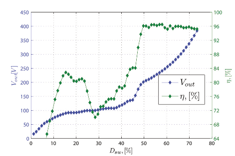
  • In order to measure the efficiency during start-up of the parallel primary prototype, the duty-cycle was gradually increased from zero to 74%.
  • Figure 12 shows the resulting efficiency measurements, as well as the measured output voltage at each duty cycle.
  • Both prototypes have a peak efficiency above 96% at the rated power, thus demonstrating the possibility of achieving high efficiency with the presented integration method.
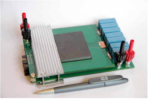
  • The parallel primary prototype is shown in fig.
  • Copper, 8 layer PCBs, with the two fullbridges mounted directly to each primary winding to minimize stray inductance.

V. CONCLUSION

  • The presented start-up method effectively addresses the start-up issue of isolated boost converters, potentially paving the way for increased industry adoption of this highly promising topology family, which so far has been limited by the startup issue.
  • The experimental work presented has focused on fuel cell applications in the kW power range, but the method may be applied to multiple other applications.
  • The constructed prototypes are hard-switched, and the fly-back mode is not optimized for high efficiency but rather for fulfilling the functional requirements of start-up without affecting normal boost mode operation efficiency.
  • Alternative applications of the method may focus on wide-range high-efficiency by employing soft-switching or regenerative snubbing, potentially making the integration method suitable for diverse applications such as Power Factor Correction and single stage inverters.

Did you find this useful? Give us your feedback

Figures (12)

Content maybe subject to copyright    Report

General rights
Copyright and moral rights for the publications made accessible in the public portal are retained by the authors and/or other copyright
owners and it is a condition of accessing publications that users recognise and abide by the legal requirements associated with these rights.
Users may download and print one copy of any publication from the public portal for the purpose of private study or research.
You may not further distribute the material or use it for any profit-making activity or commercial gain
You may freely distribute the URL identifying the publication in the public portal
If you believe that this document breaches copyright please contact us providing details, and we will remove access to the work immediately
and investigate your claim.
Downloaded from orbit.dtu.dk on: Aug 10, 2022
A New Method for Start-up of Isolated Boost Converters Using Magnetic- and Winding-
Integration
Lindberg-Poulsen, Kristian; Ouyang, Ziwei; Sen, Gökhan; Andersen, Michael A. E.
Published in:
Annual IEEE Applied Power Electronics Conference and Exposition
Link to article, DOI:
10.1109/APEC.2012.6165841
Publication date:
2012
Link back to DTU Orbit
Citation (APA):
Lindberg-Poulsen, K., Ouyang, Z., Sen, G., & Andersen, M. A. E. (2012). A New Method for Start-up of Isolated
Boost Converters Using Magnetic- and Winding-Integration. In Annual IEEE Applied Power Electronics
Conference and Exposition: Proceedings (pp. 340-345). IEEE. https://doi.org/10.1109/APEC.2012.6165841

A New Method for Start-up of Isolated Boost
Converters Using Magnetic- and
Winding-Integration
Kristian Lindberg-Poulsen
Technical University of
Denmark, Dept. of
Electrical Engineering
k.lindberg.p@gmail.com
Ziwei Ouyang
Technical University of
Denmark, Dept. of
Electrical Engineering
zo@elektro.dtu.dk
Gökhan Sen
Technical University of
Denmark, Dept. of
Electrical Engineering
gs@elektro.dtu.dk
Michael A.E. Andersen
Technical University of
Denmark, Dept. of
Electrical Engineering
ma@elektro.dtu.dk
Abstract—A new solution to the start-up and low output
voltage operation of isolated boost family converters is presented.
By the use of integrated magnetics and winding integration, the
transformer secondary winding is re-used during start-up as a
flyback winding coupled to the boost inductor. The traditional
added flyback winding coupled to the boost inductor is thus
eliminated from the circuit, bringing substantial cost savings,
increased efficiency and simplified design. Each subinterval of
the converter operation is described through electrical and
magnetic circuit diagrams, and the concept is extended to other
isolated boost family topologies. The principle of operation is
demonstrated with a 800W isolated boost prototype, and a 1600W
primary parallel series secondary isolated boost converter. Effi-
ciency measurements of both prototypes are presented, including
measurements during both start-up and normal boost operation.
I. INTRODUCTION
Isolated boost converters have been shown to be the most
efficient topology for high power, low input voltage, high out-
put voltage applications [1]–[5]. Suitable applications include
distributed generation systems, backup systems, fuel cell con-
verters, electric vehicle applications and avionic applications.
However, a disadvantage of the topology is that the boost
characteristic sets a lower limit for the output voltage, which
introduces in-rush current during start-up from zero output
voltage, as well as during fault situations such as output short
circuit.
Fig.1 shows a common solution to the start-up problem [6],
[7]. A flyback winding is arranged on the boost inductor, such
Fig. 1. Isolated full-bridge boost converter with traditional start-up method
using added external flyback winding and diode.
that the converter may operate as a flyback converter during
start-up with the associated buck-boost voltage modulation
factor allowing control of the output voltage all the way down
to zero volts. During normal boost operation, the flyback wind-
ing is completely inactive, but occupies part of the winding
window of the boost inductor, leaving less copper area for the
boost inductor, which in turn causes a drop in efficiency. Being
a power transferring magnetic component, the flyback winding
is a relatively expensive circuit element and complicates the
assembly of the boost inductor. Fig.2 and Fig.3 respectively
show the simplified and complete circuit diagrams of the new
circuit topology, where the magnetic integration of the boost
inductor with the transformer allows the boost inductor to
couple to the secondary winding during start-up, such that
the secondary winding acts as flyback winding.
II. PRINCIPLE OF OPERATION
Figures 4 to 7 explain the principle of operation as
applied to the basic full-bridge isolated boost topology. Each
Fig. 2. Electrical circuit diagram of new start-up method.
Fig. 3. Electrical and magnetic circuit diagram of new start-up method using
EI core with center leg air gap.
978-1-4577-1216-6/12/$26.00 ©2012 IEEE 340

subinterval of operation is shown with an electric circuit
diagram followed by the corresponding and a magnetic core
diagram. Relevant voltage polarities are marked with +/-
signs, and current directions are marked with arrows while
inactive elements are dimmed. The electric circuit diagrams
correspond to their respective core diagrams by the ports
marked a, b, c, d. The core diagrams include the flux rate,
dt
= φ
0
, induced by the inductor, as well as the flux rate
induced by the transformer. The circuit operation can be
understood by analysing voltage polarities and flux rates
together with the right hand rule, while taking into account
the switch states, current directions and diode bias.
Boost mode operation (D
sw
0.5)
In the familiar isolated boost topology, the full-bridge
switch duty cycle must be above 0.5, such that there is always
a current path available for the boost inductor. This is defined
as the normal boost mode operation. The gate signal is
phase-shifted 180
between each diagonal high-side/low-side
switch pair. Since D
sw
0.5, the phase shifted gate signals
overlap such that either all switches are on, or two diagonal
switches are on.
When all switches are on, V
in
is applied to the boost inductor,
and the input current is increasing. Known as the charging
or boosting subinterval, the circuit operation during this is
shown in fig. 4. As seen in fig. 4(b), the flux rate induced by
the inductor is uncoupled from the transformer windings due
to the fact that the voltage drops induced on the transformer
windings on each side leg are of opposite polarity.
The second sub-interval, referred to as the boost mode
discharge subinterval, is shown in fig. 5. When two diagonal
switches are on and the other two are off, the inductor
current passes through the primary winding, allowing the
corresponding diagonal diode pair of the output rectifier to
become forward biased. The output voltage is reflected to the
primary winding, such that a negative voltage drop is applied
over the inductor, decreasing the current. The corresponding
core diagram in fig. 5(b) shows that the inductor flux rate
is decreasing, and is still uncoupled from the transformer.
Additionally, it is noted that the flyback diode D
f
is reverse
biased.
Start-up mode operation (D
sw
< 0.5)
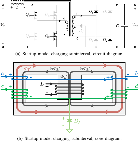
When the switch duty cycle is reduced below 0.5, the
diagonal switch pairs are no longer overlapping in on-state,
meaning that either two diagonal switches are on or all
switches are off. When two switches are on, the circuit
operation is identical to the boost mode discharge subinterval,
except that the inductor current is now decreasing due to the
fact that the primary voltage is lower than the input voltage,
causing a positive voltage drop over L. Because of this,
the subinterval is referred to as the start-up mode charging
subinterval, and the corresponding circuit and core diagrams
are seen in fig. 6.
(a) Boost mode, charging subinterval, circuit diagram.
(b) Boost mode, charging subinterval, core diagram.
Fig. 4. Boost mode, charging subinterval. All switches are on, inductor
current is increasing. Core diagram shows that inductor flux rate is decoupled
from transformer.
(a) Boost mode, discharging subinterval, circuit diagram.
(b) Boost mode, discharging subinterval, core diagram.
Fig. 5. Boost mode, discharge subinterval. Two diagonal switches are on,
inductor current is decreased by transferring energy through the transformer.
It is noted that D
f
is reverse biased..
When all switches are off, there needs to be an alternative
current path such that the inductor flux remains continuous
in order to avoid MOSFET avalanche mode clamping of the
stored energy. This current path is provided by the secondary
transformer winding, which thereby acts as a flyback winding
during the flyback discharge subinterval seen in fig. 7. During
switch turn off, the inductor current is decreasing, creating a
341

(a) Startup mode, charging subinterval, circuit diagram.
(b) Startup mode, charging subinterval, core diagram.
Fig. 6. Start-up mode, charging subinterval. Two diagonal switches are on,
charging the inductor while also transferring energy through the transformer.
reverse in the flux rate, as seen by comparing φ
0
L
on fig. 6(b)
and fig. 7(b). Following the right hand rule, it is evident that
this induces respective voltage drops over each half of the
secondary winding, with polarities such as to allow D
f
to
become forward biased. The two halves of the secondary
winding will then be working in parallel to discharge the
energy stored in the air gap, with the full output voltage
applied to each winding half.
It should be noted that it would also be possible to run the
converter in "pure flyback mode", wherein either all switches
are on or all switches are off. However, this means that
zero energy is transferred to the output during the boosting
subinterval, leading to higher current ripple at same output
power. The "hybrid" startup mode shown in figs. 6 and 7 has
been described in-depth as applied to a conventional external
flyback winding [7], and the specific timing analysis of the
previous work can be directly applied to the new integrated
magnetic approach.
III. EXTENSION TO OTHER ISOLATED BOOST FAMILY
TOPOLOGIES
The concept can readily be applied to numerous isolated
boost derived topologies, such as flyback- current-fed push-
pull [8], dual inductor [9], and parallel primary isolated boost
[3]. It can also be applied to various rectification circuits,
including voltage doubler and center tap rectifier. Figure 8
shows the principle applied to an isolated boost converter with
a center tap rectifier. In this case, the flyback diode D
f
is no
longer required, and the start-up functionality is gained "or
free" using only the specified integrated magnetic structure,
which may be beneficial in itself by reducing magnetic com-
(a) Startup mode, discharging subinterval, circuit diagram.
(b) Startup mode, discharging subinterval, core diagram.
Fig. 7. Start-up mode, flyback discharge subinterval. All switches are turned
off. The drop in inductor current causes a reverse in the associated flux rate,
which couples to the secondary transformer windings. From the polarity of
the induced voltages, it is evident that this allows D
f
to be forward biased,
such that the energy stored in the air gap can be discharged to the converter
output.
Fig. 8. New start-up method applied to isolated boost with center tap
rectification circuit, where a flyback diode is not required.
ponent count and increasing efficiency [10]. Figure 9 shows
the principle applied to the parallel primary topology, which
has been shown to be an efficient way of scaling isolated boost
converter design for higher power [3], [4]. Additionally, the
shown implementation features a shared center leg for flux
cancellation, resulting in increased efficiency [11]. It is noted
that only a single flyback diode is required, regardless of the
degree of paralleling.
Additional applications include dual inductor isolated boost
and Weinberg/push-pull isolated boost topologies.
IV. EXPERIMENTAL VERIFICATION
An 800W isolated boost prototype as well as a 1600W
parallel primary isolated boost prototype have been built
in order to verify the start-up functionality, as well as to
demonstrate the possibility of achieving high efficiency and
high power density by application of the integration method.
Both converters are hard-switched, and rely on extensive
interleaving to achieve a low transformer leakage inductance
342

Fig. 9. New start-up method applied to parallel primary isolated boost
topology.
of 91nH and 124nH respectively. The converters are designed
for fuel-cell application, where a fuel cell output voltage of
25-35V is expected.
Figure 11 shows current measurements during start-up mode
of the isolated boost prototype. The converter is running at
V
in
= 25V , D
sw
= 40%, V
out
= 60V and 100Ω load. C3
(blue) shows the AC component of the input current, C4(green)
shows the AC component of the current through a high side
output rectifier D
1
, while C1(yellow) and C2(red) show the
two gate signals.
When the gate signal C1(yellow) is high, D
1
and D
3
are
forward biased, conducting a constant current through the
secondary winding to the load. During this period, the boost
inductor current C3(blue) is rising. After C1(yellow) goes to
zero, all MOSFETs are turned off, and the boost inductor
current quickly drops. At this moment, current continues
flowing through D
1
, safely discharging the energy stored in
the boost inductor to the output. In fig. 11, C4(green) shows
the current of the flyback diode D
f
, clearly demonstrating the
commutation of the boost inductor current.
Fig. 10. Currrent waveforms of isolated boost prototype during startup mode.
C3 (blue) shows the AC component of the input current, C4(green) shows the
current through a high side output rectifier D
1
, while C1(yellow) and C2(red)
show the two gate signals.
Fig. 11. Currrent waveforms of isolated boost prototype during startup mode.
C3 (blue) shows the AC component of the input current, C4(green) shows the
current through the flyback diode D
f
, while C1(yellow) and C2(red) show
the two gate signals.
A. Efficiency Measurements
In order to measure the efficiency during start-up of the par-
allel primary prototype, the duty-cycle was gradually increased
from zero to 74%. A fixed load of 100Ω is used across the
range, corresponding to the rated 1600W at V
out
= 400V .
Figure 12 shows the resulting efficiency measurements, as
well as the measured output voltage at each duty cycle. The
local maximum of efficiency around D
sw
= 20% is caused
by discontinuous conduction mode. Close to D
sw
= 50%, the
efficiency rises dramatically, as an increasingly greater propor-
tion of the total power is transferred through the transformer
rather than the flyback operation. The converter is capable of
operating continuously in start-up mode without overheating,
and the voltage transitions smoothly across D
sw
= 50%.
The efficiency during normal operation was measured for
both the 800W isolated boost prototype and the 1600W
parallel primary. Figure 13 shows the isolated boost prototype
measurements, while fig. 12 shows the results for the parallel
primary prototype. Both prototypes have a peak efficiency
Fig. 12. Efficiency measurements of parallel primary prototype, showing
efficiency and output voltage as a function of duty cycle, with a fixed load
of 100Ω.
343

Citations
More filters
Journal ArticleDOI
TL;DR: In this paper, a modulation technique for the bidirectional operation of the phase-shift full-bridge (PSFB) dc/dc power converter is proposed to overcome the drain voltage overshoot of the isolated boost converter, without additional components other than the ones in a standard PSFB.
Abstract: This paper proposes a novel modulation technique for the bidirectional operation of the phase-shift full-bridge (PSFB) dc/dc power converter. The forward or buck operation of this topology is well known and widely used in medium-to-high-power dc-to-dc converters. In contrast, backward or boost operation is less typical since it exhibits large drain voltage overshoot in devices located at the secondary or current-fed side—a known problem in isolated boost converters. For that reason, other topologies of symmetric configuration are preferred in bidirectional applications. In this work, we propose a modulation technique overcoming the drain voltage overshoot of the isolated boost converter, without additional components other than the ones in a standard PSFB and still achieving full or nearly full ZVS in the primary or voltage-fed side devices along all the load range. The proposed modulation has been tested in a bidirectional 3.3 kW PSFB achieving a 98% of peak efficiency in buck mode (380 V input, 54.5 V output), and a 97.5% in boost mode (51 V input, 400 V output). This demonstrates that the PSFB converter may become a relatively simple and efficient topology for bidirectional dc-to-dc converter applications.

25 citations


Cites background from "A new method for start-up of isolat..."

  • ...Some alternatives have been already proposed in the literature: when the bidirectional PSFB is part of a full ac/dc multistage converter, it would be possible to integrate the charging up of the bulk capacitance from the ac/dc stage whenever the ac grid voltage is present, like for example in photovoltaic applications; some other alternatives require additional auxiliary circuitry [16], [25], [26]....

    [...]

Journal ArticleDOI
TL;DR: A new startup strategy is proposed to make the peak transformer current in the charging process a constant value, indicating that the strategy is insensitive to initial values.
Abstract: Solid-state transformer (SST) is widely used in many fields and it plays a key role in the development of energy internet. The startup strategy of SST adopted in distribution network has to be designed elaborately because in this application the requirement of functionality, flexibility, and expandability is very high. A number of researches for the startup process of SST were made and several solutions were proposed. In these solutions, the transformer current in the charging process was unable to be observed or controlled, leading to the lack of analytical basis in a startup strategy design. In order to make the charging process observable and controllable, the authors developed a mathematical model of this process. Based on the model, a new startup strategy is proposed to make the peak transformer current in the charging process a constant value. Cases with different conditions are analyzed, indicating that the strategy is insensitive to initial values. Experimental results are provided to validate the accuracy of the mathematical model and the effectiveness of the presented solution.

13 citations


Cites methods from "A new method for start-up of isolat..."

  • ...[19] used magnetic and winding integrations for the startup charging and eliminated the added flyback winding coupled to the boost inductor....

    [...]

Proceedings ArticleDOI
01 Oct 2013
TL;DR: This paper analyses how the fuel cell I-V characteristics influences the power electronics converter efficiency and their consequence on the overall system including the most suitable control strategy which maximizes the dc-dc conversion efficiency.
Abstract: Renewable energy sources are fluctuating depending on the availability of the energy source For this reason, energy storage is becoming more important and bidirectional fuel cells represent an attractive technology Fuel cells require high-current low-voltage dc-dc or dc-ac converters as power interface to the grid In power electronics, the converter efficiency is characterized at fixed operating voltage for various output power This type of characterization is not suitable for fuel cells, since as the power from the fuel cell increases, the cell voltage decreases This paper analyses how the fuel cell I-V characteristics influences the power electronics converter efficiency and their consequence on the overall system A load-dependent efficiency curve is presented based on experimental results from a 6 kW dc-dc converter prototype including the most suitable control strategy which maximizes the dc-dc conversion efficiency

11 citations


Cites background from "A new method for start-up of isolat..."

  • ...Several solutions have been proposed to solve this issue [7][8] however, the selected system topology is not affected by this issue since the control loop of the grid tie inverter maintains the high voltage bus in the specified range....

    [...]

Proceedings ArticleDOI
11 Oct 2020
TL;DR: A generalized DCX modulation scheme is proposed in this paper to maximize the average DCX output current and to enable soft startup transitions in the two configurations considered.
Abstract: In a composite dc-dc converter, regulation and dual active bridge (DAB)-based fixed-ratio (DCX) modules are arranged to minimize stresses and losses over wide ranges of input and output voltages. The system relies on smooth mode transitions in which a DCX must be quickly powered up from zero output to its nominal fixed-ratio operation. In the case a DCX precedes a regulation stage, the DCX is exposed to a high input voltage, leading to a large inrush current during startup. In the case a DCX follows a regulation stage, the DCX needs to charge the output dc capacitor while simultaneously supplying a high load current. To address these challenges, a generalized DCX modulation scheme is proposed in this paper to maximize the average DCX output current and to enable soft startup transitions in the two configurations considered. The approach is verified by simulations and by experimental results on a 350 V, 25 kW SiC-based prototype.

4 citations


Cites methods from "A new method for start-up of isolat..."

  • ...DCX soft startup strategies presented in previous works can generally be classified into the following two types: 1) introducing auxiliary charging resistors [3] or charging circuits [4], [5], which complicates the power stage, and may compromise power density, efficiency, or speed of mode transitions; 2) limiting volt-seconds applied to Lr by applying a custom modulation scheme to the existing full-bridge switches [6]– [9]....

    [...]

Dissertation
19 Jun 2015
TL;DR: In this article, an additional transitional stage is proposed to reduce the current spike without the use of any additional components, and the active clamp not only helps eliminate the transient spike caused by the transformer leakage, but also continues to be used during steady state.
Abstract: The bi-directional dc/dc converter is a very popular and effective tool for alternative energy applications. One way it can be utilized is to charge and discharge batteries used in residential solar energy systems. In the day, excess power from the PV panels is used to charge the batteries. During the night, the charged batteries will power the dc bus for loads in the house such as home appliances. The dual active bridge (DAB) converter is very useful because of its high power capability and efficiency. Its symmetry is effective in transferring power in both directions. However, the DAB converter has drawbacks in the start-up stage. These drawbacks in boost mode include high in-rush current during start-up, and the fact that the high side voltage cannot be lower than the low side voltage. A popular existing method to alleviate this problem is the use of an active clamp and a flyback transformer in the circuit topology to charge the high side before the converter is switched into normal boost operation. The active clamp not only helps eliminate the transient spike caused by the transformer leakage, but also continues to be used during steady state. However, this method introduces a new current spike occurring when the converter transitions from start-up mode to boost mode. To alleviate this new setback, an additional transitional stage is proposed to significantly reduce the current spike without the use of any additional components. The converter is current-fed on the low side, and voltage-fed on the high side. A simple phase shif

3 citations


Cites background from "A new method for start-up of isolat..."

  • ...Additionally, the wide range of frequencies the components in the converter must be operational in leads to costlier and more complex components [27, 28]....

    [...]

References
More filters
Proceedings ArticleDOI
01 Nov 2009
TL;DR: In this paper, a 10 kW isolated R4 boost converter for low-voltage high-power fuel cell applications is presented using a new concept for partially paralleling of isolated boost converters, only the critical high ac current parts are paralleled.
Abstract: A new very high efficiency 10 kW isolated R4 boost converter for low-voltage high-power fuel cell applications is presented Using a new concept for partially paralleling of isolated boost converters, only the critical high ac-current parts are paralleled Four 25 kW power stages, consisting of full-bridge switching stages and power transformers, operate in parallel on primary side and in series on secondary side Current sharing is guaranteed by series connection of transformer secondary windings and three small cascaded current balancing transformers on primary side The detailed design of a 10 kW prototype converter is presented Input voltage range is 30–60 V and output voltage is 800 V Test results, including voltage- and current waveforms and efficiency measurements, are presented A record high converter efficiency of 982 % is achieved The proposed R4 boost converter thus constitutes a low cost solution to achieve very high conversion efficiency in high input current applications

18 citations


"A new method for start-up of isolat..." refers background in this paper

  • ...Figure 9 shows the principle applied to the parallel primary topology, which has been shown to be an efficient way of scaling isolated boost converter design for higher power [3], [4]....

    [...]

Proceedings ArticleDOI
06 Mar 2011
TL;DR: In this paper, a planar integrated magnetics (PIM) design approach for primary parallel isolated boost converters is presented, where all magnetic components in the converter including two input inductors and two transformers with primary-parallel and secondary-series windings are integrated into an E-I-E core geometry.
Abstract: A high efficient planar integrated magnetics (PIM) design approach for primary parallel isolated boost converters is presented. All magnetic components in the converter including two input inductors and two transformers with primary-parallel and secondary-series windings are integrated into an E-I-E core geometry. Due to a low reluctance path provided by the shared I-core, the two transformers as well as the two input inductors can be integrated independently, reducing the total ferrite volume and core loss. AC losses in the windings and the leakage inductance of the transformer are kept low by interleaving the primary and secondary turns of the transformers. To verify the validity of the design approach, a 1-kW prototype converter with two primary power stages is implemented for a fuel cell fed battery charger application with 20–40 V input and 170–230 V output. An efficiency of 96% can be achieved during nominal operating conditions. Also experimental comparisons between the PIM module and two separate cases have been done in order to illustrate the advantages of the proposed method.

15 citations

Proceedings ArticleDOI
01 Nov 2010
TL;DR: In this article, a planar integrated magnetics (PIM) technique for a phase-shift plus duty cycle controlled hybrid bi-directional DC/DC converter is presented and investigated, where the main magnetic components including one boost inductor and two independent transformers are integrated into an E-I-E core geometry.
Abstract: In the most power electronics converters, the overall volume is mainly determined by the number of parts and the size of passive components. Integrated magnetics and planar magnetics techniques therefore have been an excellent option in order to reduce the count and the size of magnetic components, hereby increasing the power density of converters. A new planar integrated magnetics (PIM) technique for a phase-shift plus duty cycle controlled hybrid bi-directional DC/DC converter is presented and investigated in this paper. The main magnetic components including one boost inductor and two independent transformers are integrated into an E-I-E core geometry. Utilizing the flux cancellation as the principle of uncoupling, the transformers and the boost inductor are integrated, to reduce the total ferrite volume and core loss. The transformers and inductor are wound in the outer legs and the center legs respectively. The uncoupling effect between them is determined by the winding connections. The middle I-core provides a shared low reluctance flux path, uncoupling the two independent transformers. With the air gaps shift into the center legs, the magnetizing inductance of transformers will not be decreased due to there is no air gap throughout the flux paths generated by the two transformers. The new PIM structure can be extended to other topologies. To verify the validity of design approach and theoretical analysis, a lab prototype with PIM has been built, and tested. Comparing with the discrete structure, the result demonstrated a great improvement in profile and volume without sacrificing electrical performance.

14 citations


Additional excerpts

  • ...ponent count and increasing efficiency [10]....

    [...]