


Noiseless, kilohertz-frame-rate, imaging detector based on micro-
channel plates readout with the Medipix2 CMOS pixel chip
Jason McPhate
*a
, John Vallerga
a
, Anton Tremsin
a
, Oswald Siegmund
a
,
Bettina Mikulec
b
, Allan Clark
b
a
Univ. of California, Berkeley, Space Sciences Laboratory, Berkeley, CA, USA 94720-7450;
b
Univ. of Geneva, DPNC, 24 quai Ernest-Ansermet, CH – 1211 Geneva 4
ABSTRACT
A new hybrid imaging detector is described that is being developed for the next generation adaptive optics (AO) wave-
front sensors. The detector consists of proximity focused microchannel plates (MCPs) read out by pixelated CMOS
application specific integrated circuit (ASIC) chips developed at CERN (“Medipix2”). Each Medipix2 pixel has an
amplifier, lower and upper charge discriminators, and a 14-bit counter. The 256 x 256 array can be read out noiselessly
(photon counting) in 286 µs. The Medipix2 is buttable on 3 sides to produce 512 x (n*256) pixel devices. The readout
can be electronically shuttered down to a temporal window of a few microseconds with an accuracy of 10 ns. Good
quantum efficiencies can be achieved from the x-ray (open faced with opaque photocathodes) to the optical (sealed tube
with multialkali or GaAs photocathode).
Keywords: Photon counting, noiseless, microchannel plate, Medipix, high frame rate, imaging, detector
1. INTRODUCTION
Advances in adaptive optic (AO) systems for ground based telescopes are placing ever more stringent requirements on
the wavefront sensor (WFS) components of these systems. In particular, the push toward larger telescopes requires AO
systems with many more actuators, each requiring a wavefront phase measurement. To accommodate the growing
number of phase elements, WFS for the next generation of giant telescopes will have to grow accordingly. The ideal
WFS
1
would have many image elements (512 x 512 pixels), very low read noise (3 electron), operate at kilohertz
frame rates, and have high optical and near infrared (NIR) quantum efficiencies (80%).
Typically WFS have employed charge coupled devices (CCDs) because of their excellent optical/NIR quantum effi-
ciency (QE). However, as WFS get larger, with more pixels per phase element to accommodate larger telescopes, the
“read noise” associated with the analog to digital conversion of the charge collected in each pixel of a CCD becomes a
significant penalty. Newer advances in CCD technology (such as massively parallel readouts
2
or on-chip structures that
amplify the collected charge before the analog to digital conversion
3
) mitigate this penalty, but cannot entirely eliminate
it.
Unlike charge integrating arrays (e.g., CCDs) photon counting detectors register each photon as a single count and so
have no “read noise”. Examples of such devices include avalanche photodiodes (APDs) and imaging microchannel
plate (MCP) detectors. While silicon based APDs are fast and have high QE in the optical and near infrared (IR) they
have not been incorporated into large arrays. Imaging MCP detectors
4
can have large areas (100 x 100 mm), high spa-
tial resolutions (25 µm FWHM), low background rates, and event timing resolution less than 1 ns. Their QE is deter-
mined by the photocathode that absorbs the incident photon and releases the photoelectron. Recent advances in gallium
arsenide (GaAs) and gallium arsenide phosphide (GaAsP) photocathodes for image intensifier devices have resulted in
optical/NIR QEs exceeding 50%
5
. Bolstered by this advance in optical/NIR photocathode technology we are actively
developing a MCP-based, photon counting WFS detector with a GaAs photocathode
6
.
Most photon counting, imaging MCP-based detectors use readout schemes that are inherently serial in nature. For in-
stance, a delay line anode which uses the difference in arrival times of an event signal at each end of the anode to calcu-
*
mcphate@ssl.berkeley.edu; phone 1 510-643-8242

late the event position, can only have one signal on the anode at a time else there is a confusion of events. With typical
delay times of 50 ns for larger detectors dead time associated with “pulse pileup” starts to become significant at global
rates as low as 2 MHz. The obvious way to avoid this problem is to use a more parallel readout structure (a pixelated
counting device) behind the MCPs. The AO WFS detector we are developing uses just such a device, allowing us to
maintain the “noiseless” readout of photon counting, while operating at global counting rates approaching 5 GHz and
frame rates of a kilohertz. For a detailed comparison of the performance characteristics as a WFS of the photon count-
ing MCP/Medipix detector discussed here verses state-of-the-art CCDs see reference 7.
2. A NOVEL DETECTOR DESIGN
Our novel detector scheme employs a CMOS application specific integrated circuit (ASIC) pixelated counting device to
readout the MCPs. Specifically, we are using the “Medipix2”
8
device, an ASIC designed and constructed by the Mi-
croelectronics Group at CERN for the multi-national MEDIPIX collaboration (http://www.cern.ch/medipix), which we
have joined. The members of the consortium have input into the features that will be present in future versions of the
Medipix ASIC and share the large costs associated with devel-
oping and fabricating a new ASIC.
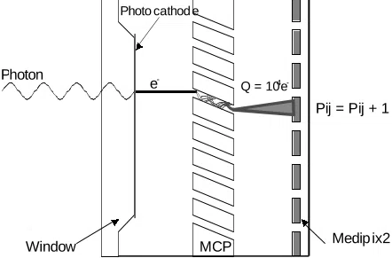
The detector (Figure 1) is a vacuum sealed MCP imaging tube
with a semi-transparent GaAs photocathode on the entrance
window and a Medipix2 readout chip. A photon interacting
with the photocathode produces a photoelectron which is prox-
imity focused onto the input surface of the MCP. The MCP
amplifies this single photoelectron with a gain on the order of
10
4
. The resultant charge cloud exits the MCP and lands on an
input pad of the Medipix2 pixel where it is counted as one
event. The Medipix2 pixel counters integrate until they are
readout in a digital, noiseless process. Also because the data is
digital, it can be read out at a fast clocking speed, allowing the
entire frame to be read out in 286 µs. This detector should
achieve optical/NIR QEs of approximately 35% (the photocath-
ode QE mitigated by the open area ratio of the MCP).
To verify that the Medipix2 device was a viable readout device
for an MCP detector we developed a photocathodeless, open-
face, MCP detector with a Medipix2 readout. Stimulation was performed primarily with UV light from a Hg penray
lamp. This detector works very well and has allowed us to experiment and optimize detector parameters such as the
MCP to Medipix gap and the accelerating voltage across this gap, important parameters for the final sealed tube design.
We were able to use this detector to perform rudimentary verification that the MCP/Medipix combination will work as a
Shack-Hartmann type WFS. We have also used the detector to detect low energy beta particles. Results obtained from
this developmental detector have been previously published
6,9
. The knowledge acquired from this developmental detec-
tor has been used to determine the parameters of the optical tube design presented in Section 3.
2.1 The Medipix2 ASIC
The Medipix2 is a pixel detector readout chip consisting of 256 x 256 identical 55 x 55 µm pixel elements, each work-
ing in single photon counting mode. Each pixel consists of a preamplifier, a discriminator, and a 14-bit pseudo-random
counter (Figure 2). The counter logic, based on a shift register, also behaves as the input/output register for the pixel.
Each cell has an 8 bit configuration register which allows masking, testing, and 3-bit individual threshold adjust for the
discriminator. Figure 3 shows the electrical schematic of the Medipix2 layout and how the shift registers relate to the
parallel readout. The total active area of the chip is 2.0 cm
2
and is 3-side buttable (supporting larger, 512 x [n*256],
arrays) with 127 wirebond output/input pads along the inactive edge. The application of the Medipix2 for this detector
has been discussed in greater detail previously
6
. Here we concentrate on the implementation using the Medipix2 as a
readout in an MCP imaging tube.
P
hoton
e
-
Q = 10
4
e
-
Pij = Pij + 1
Window
Medipix2
MCP
Photocathode
Figure 1: Schematic of a sealed tube MCP imager using
a Medipix2 ASIC for readout. Each detected photon
results in a single count increment in pixel Pij.

Readout of the Medipix2 chip can be performed via either a serial or a parallel interface. Upload to the chip is per-
formed with a serial interface. Both serial and parallel interfaces are clocked by a fast external clock (up to 100 MHz).
The serial input and output employ low voltage differential signal (LVDS) line pairs. The fast clock, for example, is
brought into the chip via a LVDS line pair. In serial mode full 256 x 256 x 14-bit frame can be read in ~9.2 ms using a
100 MHz clock. The parallel readout is a 32-bit CMOS bus
that outputs each 256 x 1-bit row of a frame in eight reads. A
100 MHz clock speed results in a parallel full frame read time
of 286 µs.
2.2 Microchannel plates
Microchannel plates consist of an array of holes in a specialized
glass substrate whose surface has a high secondary electron
coefficient. When biased with a high voltage across the plate,
electron(s) entering a pore are accelerated and eventually im-
pact the channel wall, releasing more electrons which continue
the process resulting in an avalanche of electrons exiting the
rear surface. Typical gains (electrons out/ electrons in) for a
single MCP range up to 5 x 10
4
, depending on the voltage ap-
plied and the length to diameter (L/d) ratio. For the relatively
low gain 10
4
we use for the MCP/Medipix detector either a sin-
gle MCP with high L/d ratio or a “chevron” pair can be used
(two MCPs stacked with their pore bias angles reversed at the
interface). The advantage of the chevron is that any ions gener-
ated in the residual gas of the tube at the MCP output cannot be
accelerated back to the photocathode, possibly damaging it.
They would be absorbed in the first MCP because of the “bend”
at the interface. We have chosen to use a chevron stack of
10 µm pore diameter MCPs for the Medipix imaging tube.
Input
Preamp
Disc.
Disc.
logic
Mux.
13 bit
counter –
Shift
Register
Clock out
Shutter
Lower Thresh.
Disc.
Mux.
Previous Pixel
Mask bit
Analog
Digital
Upper Thresh.
Next Pixel
Mask bit
Polarity
Figure 2: Schematic of the major functional blocks contained within
a Medipix2 pixel. A fast charge event on the input is amplified and
shaped by the preamp, discriminated, and counted at the shift regis-
ter (if Shutter is disabled). The digital number count is clocked out
at high rate through the shift registers of the pixel column when
Shutter is enabled. Digital configuration bits are input through this
same shift register to control thresholds, masking, and electrical
testing.
Figure 3: Schematic of the readout architecture of the
Medipix2 chip organized into 3328 bit columns read
out via a 256 bit fast shift register with a 32 bit parallel
readout.
Figure 4: Image of the input face of a Medipix2 chip.
The dimensions are 1.6 cm high and 1.4 cm wide. The
active area has 256 x 256 pixels and is buttable on 3
sides. Inactive bottom edge has input/output wirebond
pads.

2.3 High QE photocathodes in the optical
GaAs photocathodes have been used extensively
for a number of years, mainly in night vision ap-
plications as the photocathode for Generation III
image intensifiers. During that time many ad-
vances in performance have been achieved. As
demonstrated in Figure 5, quantum efficiencies in
excess of 50% can now be achieved from 550 nm
to 850 nm making them very attractive for opti-
cal/NIR astronomical applications. However,
these photocathodes are extremely environmen-
tally sensitive and must be kept at ultrahigh vac-
uum to prevent QE degradation. They are depos-
ited on windows and built into vacuum tubes con-
structed to seal and maintain vacuum levels of 10
-9
Torr or better. Furthermore, production of reliable
GaAs photocathodes is expensive to implement,
so working with an established volume production
facility is important.
3. OPTICAL MCP/MEDIPIX IMAGING DETECTOR DESIGN
Although the approach of using a volume supplier of GaAs devices to process the photocathode greatly reduces the cost
of achieving high QE imaging device it places significant constraints on the detector design. In particular our vacuum
tube and entrance window must be compatible with the fixtures of the production facility, effectively dictating the use
of a standard size tube and window. The interior of a standard night vision type vacuum tube is only marginally larger
than the Medipix2 device, making space constraints inside the vacuum tube very restrictive. Also the sensitivity of the
photocathode to contamination means that everything that goes into the tube must be extremely low outgassing.
The Medipix2 device also places significant constraints on the design. The input/output contact pads of the Medipix are
primarily along one edge and are spaced on a 120 µm pitch. About half of the 127 contacts on the Medipix need to be
brought out of the vacuum, requiring a relatively fine spacing of contacts and dense population of hermetic vias on the
header to which the Medipix is bonded. Also the readout rates we wish to achieve require attention be given to imped-
ance matching and power and ground filtering on the Medipix header. Add to all this the requirement that the header
and die bond material must be able to withstand the temperatures (~300 ºC) reached during the vacuum tube processing
while still being extremely low outgassing to avoid photocathode degradation.
Achieving good spatial resolution requires a relatively small gap between the photocathode surface of the window and
the input face of the MCPs. To keep the MCP output charge cloud spread to a minimum the gap between the MCPs and
the Medipix must also be minimized. Both of these affect the allowable stack up tolerance of the piece parts of the tube
body as well as the tolerance on the braze line thicknesses between parts. The MCP to Medipix gap also constrains the
maximum permissible wirebond loop height. Externally controlled high voltage potentials need to be applied across the
photocathode to MCP gap (improves spatial resolution), the MCP input to output surfaces (controls MCP gain), and the
MCP to Medipix gap (minimizes charge cloud spreading). All these requirements lead to a fairly standard metal ce-
ramic brazed body tube assembly with tight stack up tolerances, employing a drop faced entrance window and having a
rather complex ceramic thick-film hybrid header for mounting the Medipix readout device (Figure 6 and Figure 7).
3.1 Medipix header
At the heart of the MCP/Medipix imaging tube is the mounting header for the Medipix2 chip. Internally this header
provides the mounting surface and electrical interface for the Medipix2 chip and externally functions as the signal inter-
face to the readout electronics. It must provide a hermetic seal on the vacuum tube while getting approximately 60 in-
dividual signals from the Medipix to the outside of the tube. It must be very low outgassing and compatible with not
just tube processing temperatures, but also active vacuum brazing temperatures (~850 ºC). The interior contact pads
need to be compatible with Al wedge wirebonding with spacing close to that of the Medipix 120 µm pad pitch. For
0
10
20
30
40
50
60
200 400 600 800 1000
Bialkali (Hamamatsu)
Extended S25 (Hamamatsu)
Extended S25 (Photonis)
GaAs (ITT)
Quantum Efficiency (%)
Wavelength (nm)
Figure 5: Quantum efficiencies for commonly used optical regime
photocathodes (Sources:
www.ittnv.com, www.hamamatsu.com), and
the more recent GaAs advances
5
.

these reasons we chose to have a hybrid header made using thick-film screening technology on a ceramic substrate. We
have used this technology with great success in many of our UV photon counting detector devices
10
. The thick-film
technology provides an extremely robust final product that is compatible with active brazing. It is not, however, com-
patible with hydrogen furnace brazing as the hydrogen reduces the thick-film materials.
There are many screening/firing steps in the creation of a multilayer thick-film header such as this one. The process
begins with a bare alumina blank with laser drilled via holes. The holes are filled with a conductive material providing
an electrical path through the ceramic and a hermetic seal of the vias. After the vias are filled each subsequent material
or layer needs to be screened on and fired separately. Thick-film screening technology can provide approximately
125 µm features with 125 µm spacing (~250 µm pitch) and each metallic layer is 10-15 µm thick after firing. To more
closely match the 120 µm Medipix output pad pitch, two layers of signal traces separated by an insulating glass were
used on the inside of the header (Figure 6). Each layer of traces has 125 µm on 125 µm featuring, and the second layer
is registered with its traces over the gaps of the lower layer to provide an effective trace pitch of 125 µm. A second
layer of insulating glass is screened over the upper traces to isolate them from the final ground plane (screened beyond
the edges of the glass to make contact to the base ground plane) to which the Medipix is bonded. Each “layer” of glass
is 60 µm thick and is formed by screening and firing four separate 15 µm patterns. The insulating glass further ensures
the hermeticity of the header and all vias are covered by at least one layer of glass. Note that only the very tips of the
traces on each layer are left exposed by the glass layer above those traces. The second, upper set of traces does not
reach the edge of the lower glass, producing a stair-like cross-sectional vertical profile for the two sets of traces and
glass.
The exterior pattern provides land pads for two 34 contact, 0.8 mm pitch connectors and decoupling capacitors that will
be installed after the tube is sealed (see Section 3.2). The Medipix needs to be mounted and wirebonded to the header
before the tube can be sealed. As the Medipix will certainly not survive the ~850 ºC active braze process a lower tem-
perature method is needed to seal the header and Medipix into the tube body. The header is brazed to a kovar adapter
flange before the Medipix is installed. Later the flange/header/Medipix assembly will be laser welded into the tube
backend. The bare ceramic outer annulus on the exterior of the header provides a surface for the active brazing of the
header to the adapter flange. The edge of the header is also screened with metal. During the brazing process the braze
material will slightly overflow (“run-out”) this region, providing a continuous, low impedance ground plane from inside
to outside. The small glass patch on the exterior protects the power lines under it from being shorted by braze run-out
(as well as ensuring the seal of the vias below it). Special care was given to the 2 x 6 LVDS traces at either end. These
traces were designed (trace width, spacing, distance to ground plane, and dielectric of insulating glass) to provide as
close to 100 differential impedance for each LVDS pair as possible given the space and materials constraints. Fi-
nally, the use of a conductive epoxy to bond the Medipix to the uppermost ground plane provides a low inductance path
for the chip backside ground plane.
Figure 6: Ceramic hybrid thick film header design. Header diameter is 27.5 mm. (a) Interior view of the first trace layer and the
hermetic vias connecting the interior traces to the exterior connector land pads, note approximately every other via is consumed in
this layer. This layer is applied directly to the bare alumina. (b) The second layer of fingers are screened on after the application
of an insulating layer of glass and make contact to the unused ceramic vias through holes in the glass. (c) The header is completed
by application of another layer of insulating glass and finally a ground plane layer is screened over this glass. The Medipix2 chip
is die bonded to this “upper” ground plane and the signal pads are Al wedge wirebonded to the exposed tips of the header traces
(cf., Figure 11). (d) Exterior view, showing the land pads for two 34 contact 0.8 mm pitch connectors and decoupling capacitors.
a
b
c
d