All figures (23)

Fig. 18. Experimental results of capacitor voltages with discharging resistor employed. (a) RP is connected in SM1. (b) RP is connected in SM6. 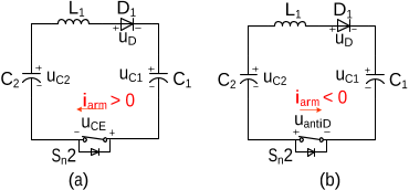
Fig. 11. The voltage distribution in balancing loop when: (a) iarm > 0, (b) iarm < 0. 
TABLE II COMPARISON OF MMC AND DCM2C 
Fig. 14. Experimental results of capacitor voltages in phase a. (a) Upper arm, 
Fig. 12. Three-phase DCM2C prototype. 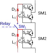
Fig. 13. Using relays to enable or disable the balancing-branches. 
TABLE III PARAMETERS OF THE PROTOTYPE 
Fig. 1. Generalized multilevel converter (one phase leg, five-level). 
Fig. 4. Balancing diagrams of Marx multilevel converter. (a) Balancing circuit. (b) Simplified circuit. 
Fig. 5. Voltage and current curves during the charging or discharging process in the Marx multilevel converter. 
Fig. 3. Deriving Marx converter from the generalized multilevel topology. 
Fig. 2. Deriving MMC from the generalized multilevel topology. 
Fig. 16. Experimental waveforms of voltage and current with S32 switching on and off, including SM capacitor voltage uC2, uC3 and current iD2. 
Fig. 17. Using RP to be connected in SM1or SM6 to increase the loss difference. 
Fig. 15. MMC and DCM2C efficiency curves vs. power. 
Fig. 8. The voltage and current diagrams of the equivalent capacitor during the discharge process. (a) Non-oscillatory discharge. (b) Damped oscillation discharge. 
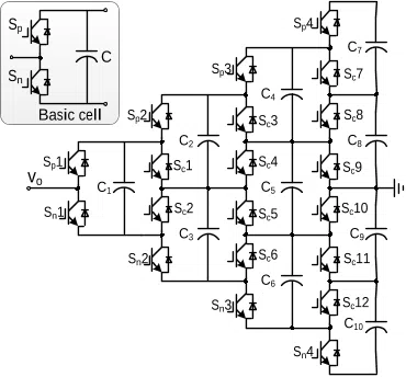
Fig. 6. The topology of three-phase DCM2C. 
Fig. 7. Balancing diagrams of DCM2C. (a) Balancing circuit. (b) Simplified circuit. 
Fig. 9. The voltage and current diagram of the equivalent capacitor during the discharging process. 
Fig. 19. Experimental waveforms of voltage and current with sudden increase of the load. (a) SM capacitor voltages uC1~uC6, uC7~uC12. (b) Load current ia, ib and ic. (c) Arm current iu, il. (d) Current iD1 through clamping diode D1. (e) Enlarged current iD1 after putting the load into operation. (f) DC-bus voltage udc. (g) Load voltage uab. (h) Enlarged voltage uab after the load increased. 
TABLE I STATES OF CAPACITORS 
Fig. 20. Experimental waveforms of voltages and currents with: (a) 50Hz operation, and (b) 20Hz operation. 
Fig. 10. Control block diagram of DCM2C as an inverter. (a) Load voltage control. (b) Capacitor voltage balancing control. (c) Switching signal generation. (d) PSC modulation.