scispace - formally typeset
Search or ask a question
Journal ArticleDOI

A Novel Diode-Clamped Modular Multilevel Converter With Simplified Capacitor Voltage-Balancing Control

TL;DR: This paper proposes a novel diode-clamped modular multilevel converter with simplified capacitor voltage-balancing control, using low-power rating diodes to clamp the capacitor voltages of the converter.
Abstract: Multilevel converters have become very attractive for high-voltage-level power conversion in renewable power generation applications. The converter topology is an important issue in the studies of multilevel converter. Many multilevel topologies have been developed, but few of them are qualified with capacitor voltage self-balancing capability. This paper proposes a novel diode-clamped modular multilevel converter with simplified capacitor voltage-balancing control. In this topology, low-power rating diodes are used to clamp the capacitor voltages of the converter. Only the top submodule in each arm of the converter requires capacitor voltage control. Consequently, very few voltage sensors are needed for voltage control and the control computation burden is reduced greatly when the quantity of the submodules is high. A simple voltage-balancing control method with carrier phase-shifted modulation strategy is developed for this topology. Experiments based on a laboratory prototype were carried out and the results validated the capacitor-balancing performance of the proposed topology.

Summary (3 min read)

Introduction

  • Attractive for high voltage-level power conversion in renewable power generation applications.
  • Experiments based on a laboratory prototype were carried out and the results validated the capacitor balancing performance of the proposed topology.
  • Its modularity and scalability enable it to meet any voltage level requirement [25]-[27].
  • From this generalized multilevel converter topology, several other multilevel topologies can be derived including the diode-clamped, capacitor-clamped, cascaded H-bridge, Marx and modular multilevel topologies [39].
  • Experimental validations of the proposed DCM2C are presented in Section IV.

A. Topology of the proposed DCM2C

  • The generalized multilevel converter was proposed as a primary multilevel topology and many other multilevel topologies can be derived from it.
  • Meanwhile the capacitor voltages are clamped by switches Sc1-Sc12.
  • Compared with the MMC, the Marx multilevel converter uses an extra switch in each SM to realize the capacitor voltage balancing without the requirement of voltage sensors and complicated control methods [40].
  • Vj, j=a, b, c, are the modulation signals of the three phase-legs.

A. Analysis of the balancing circuit

  • In practical operation, both the clamping diode and switch have the forward on voltage, which should be taken into account, especially when n is high.
  • (12) 2) iarm < 0: The negative current flows through the antiparallel diode in the switch and the voltage drop equals the diode forward on voltage uantiD. Fig. 11 (b) shows the voltage distribution diagram in this case.
  • Generally the power flowing through the balancing circuit equals half of the power difference between the two SMs.
  • Thus the current rating of the clamping diode can be very low, e.g. 10% of that of the main switch.
  • High current pulses may appear in the recovery from a serious imbalance.

B. Discussion on DCM2C losses

  • The loss of MMC is consumed by the power switches, parasitic resistance and control circuits.
  • Since the last two parts account for so small proportion of the total losses that they can be neglected, only the power switch loss is investigated.
  • PaD mainly contains the conduction loss PaDcon and recovery loss PaDrec.
  • The current flowing through the clamping diode is much lower than the arm current.

C. Device requirements of MMC and DCM2C

  • Table II lists the main device requirements of MMC and DCM2C.
  • Regardless of the devices which possess the same cost in the two converters, such as the power switches and storage capacitors, the cost difference is mainly related to the clamping diodes, inductors, voltage sensors and capacitor voltage measuring circuit.
  • The DCM2C requires more power diodes and inductors than the MMC, but much fewer voltage sensors and measuring circuits.
  • Additionally, the current rating of the clamping diode and the inductor is much lower than that of the main switches.

IV. EXPERIMENTAL RESULTS AND DISCUSSION

  • A three-phase DCM2C prototype has been developed for experiments, as shown in Fig. 12.
  • The control unit is based on DSP (TMS320F28335) and FPGA (EP3C25F324), and as many as 80 optical fibers are used to transmit switching signals, communication and fault signals.
  • Furthermore, a Tektronix scope TDS2024 is used to record the experimental data.
  • Several comparison experiments were carried out to investigate the features of this topology.

A. Experiment I: Voltage balancing verification and efficiency test

  • This experiment aims to validate the effectiveness of balancing-branches of DCM2C.
  • When the relays are closed, the balancing-branches are enabled, otherwise disabled.
  • The serious unbalanced capacitor voltages were balanced very quickly as shown in Fig. 14.
  • Remove the 2kΩ-resistors attached to SMs and: 1) Keep the relay contacts open.
  • It can be seen that the DCM2C efficiency is close to that of MMC, and both rise as the output power increases.

B. Experiment II: Balancing process in detail

  • This experiment aims to investigate the balancing process with the switch on and off.
  • A voltage deviation, as shown in Fig. 16, existed between SM2 and SM3.
  • When Sn3 switched on, the balancing current pulse appeared with a voltage deviation decrease.
  • When Sn3 switched off, the current dropped to zero.
  • The initial deviation was about 9 V and the first current peak was about 11 A. Generally the voltage deviation would not be that large in the steady operation.

C. Experiment III: Test for balancing capability

  • An experiment was carried out to test the balancing capability of the DCM2C when the loss difference between the SMs is high.
  • In fact the power resistors connected in SM1 and SM6 represent the best and worst situations for balancing performance because of the direction of the diodes.
  • The results in the two cases are presented in Fig. 18 (a) and (b) respectively.
  • As shown in Fig. 18, the capacitor voltage deviations between the maximum and minimum in (a) and (b) are about 5V and 7V respectively.
  • The capacitor voltages can still be well balanced when the power difference between SMs is high.

D. Experiment IV: Influence of the main circuit current

  • The output change may affect the capacitor voltage balance, and an experiment of sudden load change has been carried out.
  • The converter started with no load and then the load was suddenly increased as shown in Fig. 19 (b). Fig. 19 (f) shows the DC-bus voltage when increasing the load.
  • When the load was increased, the capacitor voltage had a drop of about 7 V. Before the load increase the current flowing through the clamping diode was high frequency narrow pulses with amplitude of lower than 1 A (Fig. 19 (d)).

E. Experiment V: Operation with 50Hz and 20Hz

  • This experiment aims to validate the effectiveness of the proposed topology when it operates with 50Hz and 20Hz.
  • Due to the limited channels of the scope, only some typical signals are sampled and displayed.
  • Comparing the results, it can be noted that when the operation frequency is lower, the capacitor voltage ripples become larger.
  • The voltage deviation between SM1 and SM6 also becomes bigger, but still within 5V.
  • The amplitudes of currents flowing through the clamping diode D1, D3 and D5 have no obvious variation, but the occurrence frequency of the current-bumps becomes lower.

V. CONCLUSION

  • Low power rating clamping diode and inductors are used to replace the balancing switch in Marx multilevel converter in this paper, and the diode-clamped modular multilevel converter (DCM2C) is proposed.
  • The capacitor voltage control of the converter is so simple that the computation burden is almost the same with that of the two-level converter.
  • In addition, the current rating of the clamping diodes and inductors is much lower than that of the main switches in the converter.
  • The efficiency of DCM2C is only slightly lower than the MMC’s efficiency because the extra losses of the clamping diodes are relatively small.
  • This converter can be used in high voltage and high power converting applications such as high voltage direct current transmission, wind power generation, and especially offshore wind power generation.

Did you find this useful? Give us your feedback

Figures (23)

Content maybe subject to copyright    Report

“© 2017 IEEE. Personal use of this material is permitted. Permission from IEEE must be obtained for all
other uses, in any current or future media, including reprinting/republishing this material for advertising or
promotional purposes, creating new collective works, for resale or redistribution to servers or lists, or reuse
of any copyrighted component of this work in other works.”

1
Abstract Multilevel converters have become very
attractive for high voltage-level power conversion in
renewable power generation applications. The converter
topology is an important issue in the studies of multilevel
converter. Many multilevel topologies have been developed,
but few of them are qualified with capacitor voltage
self-balancing capability. This paper proposes a novel
diode-clamped modular multilevel converter (DCMMC)
with simplified capacitor voltage balancing control. In this
topology, low power rating diodes are used to clamp the
capacitor voltages of the converter. Only the top
sub-module in each arm of the converter requires capacitor
voltage control. Consequently, very few voltage sensors are
needed for voltage control and the control computation
burden is reduced greatly when the quantity of the
sub-modules is high. A simple voltage balancing control
method with carrier phase-shifted (CPS) modulation
strategy is developed for this topology. Experiments based
on a laboratory prototype were carried out and the results
validated the capacitor balancing performance of the
proposed topology.
Index Terms Multilevel converters, diode-clamped modular
multilevel converter, capacitor voltage balancing.
I. INTRODUCTION
IGH voltage-level power conversion and transmission
have become very popular for wind power and
photovoltaic power generation, since the power scale of a wind
farm or a photovoltaic power station is becoming larger and
larger, even over hundreds of MWs. And high-voltage AC/DC
or DC/AC converters are the basic elements in such
applications. With low total harmonic distortion (THD) and
low voltage stress on power switches the multilevel converter is
a good choice for these applications.
Since 1980, multilevel converters have been developed
extensively [1]-[6]. The most famous multilevel converter
topologies are the neutral-point clamped (NPC), the
flying-capacitor (FC) and the cascaded multilevel converters. It
is easy to achieve a three- or five-level converter using the NPC
or FC topology. However, numerous clamping diodes and
capacitors are required when the voltage levels are high.
Furthermore, the capacitor voltage balancing control is difficult
and complicated [7]-[10].
With superior modularity and the least component
requirement among various multilevel topologies, the cascaded
H-bridge (CHB) multilevel converter seems to be the most
Manuscript received ******, ******This work is supported by ******.
suitable for medium-voltage active power conversion [11]-[16].
The voltage of the cells is maintained by isolated dc voltage
source, which can be supplied by wind turbine generator,
photovoltaic-cell, or windings of a multiwinding transformer,
etc. However, the requirement of isolated dc voltage supplies
and energy storage systems is the shortcoming in some
applications. When the CHB converter is applied in reactive
power conversion, e.g., STATCOM [17]-[20], the floating
capacitor voltage balancing control becomes the most
challenging issue.
Over the last decade the modular multilevel converter
(MMC) topology as another kind of cascaded topology has
gained growing attentions and found itself very attractive for
medium/high-voltage applications [21]-[24]. Its modularity and
scalability enable it to meet any voltage level requirement
[25]-[27]. However, like the CHB topology, the capacitor
voltage imbalance distributed in sub-modules (SMs) still
remains. Many researchers concentrate on developing control
and modulation strategies to solve the problem [27]-[39]. The
most widely accepted voltage balancing strategy is based on a
sorting method [27]. Li proposed an improved modulation
method to balance the capacitor voltages [28]. The control
systems rely on voltage sensors installed in all the SMs. In
addition, extra switching actions [29] [30] or high execution
frequency of voltage sorting algorithms [31] [32] are usually
involved, and the situation will deteriorate when the number of
SMs is high [33].
In 2001, Peng proposed a generalized multilevel converter
[38], which can balance each capacitor voltage automatically
without any additional circuits when applied in active or
reactive power conversion. From this generalized multilevel
converter topology, several other multilevel topologies can be
derived including the diode-clamped, capacitor-clamped,
cascaded H-bridge, Marx and modular multilevel topologies
[39]. However, the quantity of components in the general
multilevel converter is too high, which limits its applications in
high voltage-level conversion. The Marx multilevel converter
was proposed by Rodriguez and Leeb in [40], which can also
realize voltage self-balancing at the price of extra active power
switches compared with the MMC.
Based on the Marx and modular multilevel converters, this
paper proposes a new type of multilevel topology in order to
achieve a simplified capacitor voltage balancing method with
modularity and good harmonic performance. In this topology, a
low current rating diode and an inductor are used to replace the
balancing switch installed in each cell of the Marx multilevel
topology. We refer this new topology as the diode-clamped
MMC (DCM2C). In this topology the number of voltage
A Novel Diode-Clamped Modular Multilevel
Converter with Simplified Capacitor Voltage
Balancing Control
H

2
sensors is greatly reduced, and a very simple balancing control
method is developed, avoiding high-frequency sorting
algorithm and extra switching actions.
The rest of this paper is organized as follows. Section II
introduces the DCM2C circuit topology and capacitor voltage
balancing control method. The voltage drop distribution in the
balancing circuit is then investigated in section III. The power
losses and device requirement comparison of MMC and
DCM2C are also discussed in this section. Experimental
validations of the proposed DCM2C are presented in Section
IV. A conclusion is made in section V.
II. OPERATION PRINCIPLES OF DCM2C
A. Topology of the proposed DCM2C
The generalized multilevel converter was proposed as a
primary multilevel topology and many other multilevel
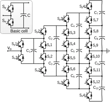
topologies can be derived from it. Fig. 1 shows one phase leg of
a five-level generalized multilevel converter and its basic cell
circuit.
v
o
Basic cell
C
1
S
p
1
S
n
1
S
p
2
S
n
2
S
p
3
S
n
3
S
n
4
S
p
4
S
p
S
n
C
C
2
C
3
C
4
C
5
C
6
C
7
C
8
C
9
C
10
S
c
2
S
c
1
S
c
4
S
c
3
S
c
6
S
c
5
S
c
8
S
c
7
S
c
10
S
c
9
S
c
12
S
c
11
Fig. 1. Generalized multilevel converter (one phase leg, five-level).
The generalized multilevel topology maintains the five-level
voltage output by switches S
p1
-S
p4
and S
n1
-S
n4
. Meanwhile the
capacitor voltages are clamped by switches S
c1
-S
c12
. For
example, when S
c1
(S
c2
) switches on, capacitor C
1
and C
3
(C
2
)
are connected in parallel. If a voltage deviation exists between
the two capacitors, balancing current will arise and flow
through the clamping switch.
The generalized multilevel topology is redundant and not
suitable for practical applications. After removing the upper
components, the MMC and the Marx multilevel converter can
be obtained, as shown in Fig. 2 and Fig. 3. Compared with the
MMC, the Marx multilevel converter uses an extra switch in
each SM to realize the capacitor voltage balancing without the
requirement of voltage sensors and complicated control
methods [40]. Taking SM1 and SM2 as examples, according to
superposition theorem, the balancing circuit and its simplified
circuit are shown in Fig. 4. C
e
is the equivalent capacitance and
R
s
is the equivalent resistance of power switch. The direction of
the balancing current i
S1
depends on the two capacitor voltage
values. The state of switch S is determined by the states of
power switch S
c1
and S
n2
(logical AND).
v
o
U
dc
Basic cell (or SM)
Fig. 2. Deriving MMC from the generalized multilevel topology.
Fig. 3. Deriving Marx converter from the generalized multilevel topology.
In Fig. 4 the circuit parameters can be derived as follows,
12
21
1
21
11
22
2
&
e
e
e
S
s
nc
C C C
u u u
u
i
R
S S S


(1)
C
2
C
1
S
n
2
i
S1
u
2
u
1
S
c
1
C
e
S
u
e
i
S1
2R
s
(a) (b)
Fig. 4. Balancing diagrams of Marx multilevel converter. (a) Balancing circuit.
(b) Simplified circuit.
t
u
e
i
C1
0
u,i
U
0
Fig. 5. Voltage and current curves during the charging or discharging process
in the Marx multilevel converter.
Fig. 5 shows the voltage and current curves of the equivalent
capacitor in the charging or discharging process. The initial
value of u
e
is U
0
. Because R
s
is usually very small, the initial
amplitude of the balancing current can be large. If the voltage
deviation between the neighboring capacitors is big, the
balancing current will be very high. This is a common
disadvantage of the traditional self-balancing multilevel
converters.
Based on the Marx multilevel converter, this paper proposes
an improved topology named as diode-clamped MMC

3
(DCM2C) to replace the extra switch with a low-current rating
diode and an inductor, which are called the balancing-branch
here. The inductor aims to suppress the peak current during the
discharging process. The clamping diodes transfer energy in
only one direction, and a simple control method is developed to
balance all the capacitor voltages in each arm. The three-phase
DCM2C topology is shown in Fig. 6. The balancing circuit and
its simplified circuit of SM1 and SM2 in the DCM2C are
derived in Fig. 7. The arm inductor L is used to limit the dc-side
short-circuit current, meanwhile as a filter for the arm current.
U
dc
S
p
1
S
n
1
C
1
S
p
(n-1)
S
n
(n-1)
C
n-1
S
p
n
S
n
n
C
n
S
p
1
S
n
1
C
1
S
p
(n-1)
S
n
(n-1)
C
n-1
S
p
n
S
n
n
C
n
v
a
v
b
v
c
SM1
SM(n-1)
SMn
SM1
SM(n-1)
SMn
A B C
Upper armLower arm
L L L
L L L
D
1
L
1
D
n-1
L
n-1
D
1
L
1
D
n-1
L
n-1
Fig. 6. The topology of three-phase DCM2C.
C
2
D
1
L
1
C
1
S
n
2
i
D1
u
2
u
1
C
e
D
1
L
1
S
n
2
i
D1
u
e
R
sum
(a) (b)
Fig. 7. Balancing diagrams of DCM2C. (a) Balancing circuit. (b) Simplified
circuit.
Equation (2) shows the parameters in the simplified circuit.
In this circuit only when u
2
> u
1
, the balancing current i
D1
can be
generated. This means that the initial capacitor voltage u
e
is
positive. R
sum
is the sum of the resistance, including R
s
of the
power switch, R
di
of the clamping diode and R
in
of the inductor.
1
21
1
1
2
e
e
sum s di in
e
D
e
CC
u u u
R R R R
u
i
R

(2)
It can be seen that this is a second-order circuit. The
differential equation and its roots, p
1
and p
2
, are expressed as (3)
and (4), respectively.
2
1
2
0
ee
e sum e e
d u du
L C R C u
dt dt
(3)
2
1
1 1 1
2
2
1 1 1
1
()
22
1
()
22
sum sum
e
sum sum
e
RR
p
L L LC
RR
p
L L LC
(4)
According to (4), there could be two cases about the relations
among the resistance, inductance and capacitance:
2
1
11
1
( ) 2
2
sum
sum
ee
R
L
R
L LC C
(5)
2
1
11
1
( ) 2
2
sum
sum
ee
R
L
R
L LC C
(6)
In the first case, p
1
and p
2
are negative real roots, and a
non-oscillatory discharging process will appear. The voltage u
e
and current i
D1
are shown in Fig. 8 (a).
In the second case, p
1
and p
2
are conjugate complex roots,
and a damped oscillation discharge process will appear. The
voltage u
e
and current i
C1
are shown in Fig. 8 (b). The balancing
current i
D1
is unidirectional due to the clamping diode. When it
drops to zero, the discharge process ends with a reversed
voltage deviation u
d
.
t
u
e
i
D1
U
0
0
u,i
t
u
e
i
D1
U
0
u
d
i
D1
=0
0
u,i
(a) (b)
Fig. 8. The voltage and current diagrams of the equivalent capacitor during the
discharge process. (a) Non-oscillatory discharge. (b) Damped oscillation
discharge.
Fig. 8 illustrates the discharge process with the power switch
S
n2
staying on all the time. Actually with S
n2
switching on and
off alternately, current pulses will be generated and the two
capacitor voltages will be balanced in several switching cycles.
Fig. 9 shows the capacitor voltage and current diagrams along
with the switching signals.
t
t
t
u
C
i
D1
u
C2
u
C1
S
n2
0
0
0
Fig. 9. The voltage and current diagram of the equivalent capacitor during the
discharging process.
In each switching cycle when S
n2
is on, D
1
and L
1
withstand a

4
voltage of u
C2
- u
C1
. If u
C2
> u
C1
, current i
D1
will arise and the
voltage deviation between the two capacitors will decrease. If
u
C1
u
C2
, no current will arise in the balancing circuit. In the
topology of DCM2C the quantity of the cascaded SMs in an
arm is n. If u
Ci+1
is higher than u
Ci
, C
i
will be charged, absorbing
energy from C
i+1
. If u
Ci+1
is lower than u
Ci
, no energy transfer
happens. As a result, the capacitor voltages of the whole arm
will be
12C C Cn
u u u
. (7)
B. Capacitor voltage balancing control
In the DCM2C topology, only one voltage sensor is required
in each arm for the balancing control, which is installed in SM1.
Six current sensors are installed in the upper arms and the lower
arms respectively, and two voltage sensors are used to measure
the load line-voltages. The upper arm currents, lower arm
currents and load voltages are i
uj
, i
lj
, u
ab
and u
bc
respectively (j =
a, b, c).
According to the relations of the arm current direction and
the SM states, the capacitor states can be achieved as listed in
Table I.
TABLE I
STATES OF CAPACITORS
Arm current
direction
SM state
Capacitor state
Positive
On
Charged
Off
Bypassed
Negative
On
Discharged
Off
Bypassed
The control strategy for the proposed converter is shown in
Fig. 10. The current control is carried out in the d-q coordinate
system. u
*
d
and u
*
q
are the voltage references. The control
variables V
j
, j=a, b, c, are the modulation signals of the three
phase-legs.
According to (7), the capacitor voltages of each arm are
clamped in a descending order from SM
1
to SMn automatically.
Assume D
dc
is the dc component of the PWM duty cycles. The
relation between the capacitor voltages and the dc bus voltage
is
,,
11
nn
dc Ci u dc Ci l dc
ii
D u D u u


. (8)
u
Ci, u
and u
Ci,l
are the capacitor voltages in the upper arm and
lower arm respectively. When the unipolar modulation strategy
is employed as shown in Fig. 10(d), D
dc
is 0.5. Then
,,
11
2
nn
Ci u Ci l dc
ii
u u u



. (9)
Furthermore, due to the symmetry of the modulation signals
for the upper arm and the lower arm, the sum of the capacitor
voltages of each arm should be
,,
11
nn
Ci u Ci l dc
ii
u u u



. (10)
Combining equation (7) and (10), if the SM1 capacitor
voltage is kept to be u
dc
/n, then all the other capacitor voltages
in this arm will be balanced as follows,
,,
dc
Ci u Ci l
u
uu
n

. (11)
A closed-loop capacitor voltage control is carried out for
each SM1, as shown in Fig. 10(b). The polarity of PI controller
output depends on the direction of arm current, according to
Table I.
abc/dq
u
ab
u
*
d
= 0
u
*
q
dq/abc
V
j
3
PI
PI
wt
wt
u
bc
(a)
u
C1,u
1/n
i
uj
Upper arm
PI
sign
u
C1,l
1/n
i
lj
PI
sign
Lower arm
V
u1, j
V
l1, j
u
dc
3
3
3
3
3
3
(b)
-1
V
j
3
S
2~n, uj
S
2~n, lj
3(n-1)
V
u1, j
V
l1, j
PSC-PWM
S
1, uj
S
1, lj
Upper
arm
Lower
arm
3
3
3(n-1)
3
3
3(n-1)
3(n-1)
SM1
SM2~n
SM1
SM2~n
(c)
θ
Triangular
carriers
Upper arm
modulation signal
Lower arm
modulation signal
t
0.5
1.0
0
(d)
Fig. 10. Control block diagram of DCM2C as an inverter. (a) Load voltage
control. (b) Capacitor voltage balancing control. (c) Switching signal
generation. (d) PSC modulation.
The PSC-PWM is applied for switching signal generation, as
shown in Fig. 10 (c). n triangular carriers with the frequency of
f
s
are assigned to the n SMs respectively. The SMs share one
modulation signal except for SM1: 1) The control variables V
j
are the common modulation signals for SM2-SMn. 2) The
output of voltage controllers V
u1,j
plus V
j
are the modulation
signals for SM1. Fig. 10(d) shows the unipolar PSC-PWM
diagram. The phase-shift angle θ is 2π/n, and the upper arm
modulation signal is opposite to that of the lower arm. The
frequency of carriers is much higher than that of the modulation
signals.
III. SPECIFIC CONSIDERATIONS FOR DCM2C
A. Analysis of the balancing circuit
In practical operation, both the clamping diode and switch

Citations
More filters
Proceedings ArticleDOI
11 Oct 2020
TL;DR: In this article, a modified Y-matrix modulation (YMM) was proposed to ensure automatic capacitor balancing for SC-MMC with a middle sub-module connecting the upper and lower arms and does not require large arm inductors.
Abstract: This paper presents a submodule (SM) capacitor voltage balancing scheme for the Switched Capacitor Modular Multilevel Converter (SC-MMC), which employs a middle submodule connecting the upper and lower arms and does not require large physical arm inductors. Only small stray/parasitic inductance is enough to limit inrush current during SM’s switching instants. This topology is directly derived from the generalized multilevel converter. The SC-MMC has the benefit of providing the same number of output voltage levels than the conventional MMC using one less submodule per phase leg. A Y-matrix modulation (YMM) that guarantees automatic SM capacitor balance without any SM feedback voltage has been proposed for an MMC topology with extremely low arm inductance. It is shown here, that the direct application of YMM cannot achieve automatic capacitor balancing for SC-MMC with middle SM. Thus, a strategy based on a modified Y-matrix modulation that requires only sensing and feedback of the middle SM voltage and output current is proposed to ensure balancing of all SM capacitor voltages. Simulation of a 6-level SC-MMC is provided to verify the voltage balancing capability with proposed control in steady state and transient conditions.

10 citations


Cites background from "A Novel Diode-Clamped Modular Multi..."

  • ...Although some substitutes, such as local dc voltage controller [4], [5], pattern swapping [6], [7], SM sorting [8], [9] and modified SM topologies [10] have been proposed, the substitutes still have drawbacks and/or limitations [11], [12]....

    [...]

Journal ArticleDOI
Yaqian Zhang1, Jianzhong Zhang1, Fujin Deng1, Zheng Xu1, Jin Zhao1 
TL;DR: An improved hybrid MMC with self-balancing branch (SBB) is proposed in this article to avoid the voltage imbalance under over-modulation situations with lower energy losses according to the comparisons with other MMC topologies.
Abstract: In the hybrid modular multilevel converter (MMC), the voltage imbalance between the capacitors of half-bridge submodule (HBSM) and full-bridge submodule (FBSM) would occur when the over-modulation index exceeds certain range, which is caused by the different charging/discharging properties of the HBSM and FBSM. An improved hybrid MMC with self-balancing branch (SBB) is proposed in this article to avoid the voltage imbalance under over-modulation situations. The SBBs could offer additional energy transmitting channel for each bypassed HBSM at the interval of negative arm voltage. Thus, the HBSMs could possess the same energy charging/discharging properties as the FBSMs, and then the voltage imbalance between the HBSM and FBSM capacitors could be avoided under any over-modulation indexes. The operation mechanism of the proposed SBB is revealed in detail, according to which the component parameter in the SBB could be selected. The effectiveness of the proposed hybrid MMC with SBBs is verified by the simulation and experimental results. Also, it shows that the proposed hybrid MMC could realize the voltage balancing under over-modulation situations with lower energy losses according to the comparisons with other MMC topologies.

9 citations

Proceedings ArticleDOI
17 Mar 2019
TL;DR: This paper mathematically proves that MMC capacitor voltage is self-balanced by nature, which implies that M MC could achieve the sub-module capacitor voltage balancing without any monitoring or control.
Abstract: The modular feature of modular multilevel converter (MMC) distinguishes itself from other topologies for medium-/high-voltage applications. However, as the count of sub-modules increases, the control complexity of voltage balancing for each sub-module sharply increases. Conventionally, the MMC is deemed to have no inherit voltage balancing property without voltage monitoring and control. This paper mathematically proves that MMC capacitor voltage is self-balanced by nature. This implies that MMC could achieve the sub-module capacitor voltage balancing without any monitoring or control. Based on the mathematical proof, a novel modulation, namely Y-Matrix Modulation (YMM), is proposed to transform the math analysis into modulation practice. With the proposed YMM, MMCs are secured self voltage balancing. Conventionally, either a complicated voltage balancing control, or extra components must be embedded to MMC to balance the capacitor voltage. Compared to conventional MMC capacitor voltage balancing strategies, YMM features extremely simple algorithms and good reachability to high-level MMCs while maintaining the original half-bridge sub-module topology.

8 citations

Journal ArticleDOI
TL;DR: Theoretical analysis shows that by introducing the integration and feedback loops of the FAC method to the conventional PIR controller, the inertia and damping effects are emerged in the system, which can help to enhance the system dynamic response during transient and achieve better suppression performance of the asymmetric components.

8 citations

Journal ArticleDOI
TL;DR: In this article , a capacitor voltage balancing method is presented for MMCs, which eliminates the need for voltage and current sensors and ensures uniform power distribution among the submodules (SMs), and it needs only one carrier per phase, and one PWM reference, for either upper arm or lower arm to produce N + 1 level with N SMs per arm.
Abstract: Modular multilevel converters (MMCs) have become prominent for high and medium power applications. The phase‐disposition pulse width modulation (PDPWM) technique is a carrier‐based method that generates good quality output. However, it has the inherent problem of uneven power distribution. Conventionally, this is solved by expensive voltage and current measurements. In this paper, a capacitor voltage balancing method is presented for MMC, which eliminates the need for voltage and current sensors. It also ensures uniform power distribution among the submodules (SMs). In addition, it needs only one carrier per phase, and one PWM reference, for either upper arm or lower arm to produce N + 1 level with N SMs per arm. The capacitor voltage balancing method is analyzed mathematically and verified for the MMC with two‐level half‐bridge SMs. The same method is also extended to the MMC with three‐level flying capacitor SMs. MATLAB/SIMULINK simulations and experimental results on a laboratory prototype are presented to verify the theoretical concepts.

7 citations

References
More filters
01 Jan 1980
TL;DR: In this article, a neutral-point-clamped PWM inverter composed of main switching devices which operate as switches for PWM and auxiliary switching devices to clamp the output terminal potential to the neutral point potential has been developed.
Abstract: A new neutral-point-clamped pulsewidth modulation (PWM) inverter composed of main switching devices which operate as switches for PWM and auxiliary switching devices to clamp the output terminal potential to the neutral point potential has been developed. This inverter output contains less harmonic content as compared with that of a conventional type. Two inverters are compared analytically and experimentally. In addition, a new PWM technique suitable for an ac drive system is applied to this inverter. The neutral-point-clamped PWM inverter adopting the new PWM technique shows an excellent drive system efficiency, including motor efficiency, and is appropriate for a wide-range variable-speed drive system.

4,432 citations

Journal ArticleDOI
TL;DR: The neutral-point-clamped PWM inverter adopting the new PWM technique shows an excellent drive system efficiency, including motor efficiency, and is appropriate for a wide-range variable-speed drive system.
Abstract: A new neutral-point-clamped pulsewidth modulation (PWM) inverter composed of main switching devices which operate as switches for PWM and auxiliary switching devices to clamp the output terminal potential to the neutral point potential has been developed. This inverter output contains less harmonic content as compared with that of a conventional type. Two inverters are compared analytically and experimentally. In addition, a new PWM technique suitable for an ac drive system is applied to this inverter. The neutral-point-clamped PWM inverter adopting the new PWM technique shows an excellent drive system efficiency, including motor efficiency, and is appropriate for a wide-range variable-speed drive system.

4,328 citations


"A Novel Diode-Clamped Modular Multi..." refers background in this paper

  • ...Since 1980, multilevel converters have been developed extensively [1]–[6]....

    [...]

Proceedings ArticleDOI
08 Oct 1995
TL;DR: This paper presents three multilevel voltage source converters: (1) diode-clamp, (2) flying-capacitors, and (3) cascaded-inverters with separate DC sources.
Abstract: Multilevel voltage source converters are emerging as a new breed of power converter options for high-power applications. The multilevel voltage source converters typically synthesize the staircase voltage wave from several levels of DC capacitor voltages. One of the major limitations of the multilevel converters is the voltage unbalance between different levels. The techniques to balance the voltage between different levels normally involve voltage clamping or capacitor charge control. There are several ways of implementing voltage balance in multilevel converters. Without considering the traditional magnetic coupled converters, this paper presents three recently developed multilevel voltage source converters: (1) diode-clamp, (2) flying-capacitors, and (3) cascaded-inverters with separate DC sources. The operating principle, features, constraints, and potential applications of these converters are discussed.

3,232 citations


"A Novel Diode-Clamped Modular Multi..." refers background in this paper

  • ...Furthermore, the capacitor voltage-balancing control is difficult and complicated [7]–[10]....

    [...]

Journal ArticleDOI
TL;DR: A general overview of the basics of operation of the MMC along with its control challenges are discussed, and a review of state-of-the-art control strategies and trends is presented as mentioned in this paper.
Abstract: The modular multilevel converter (MMC) has been a subject of increasing importance for medium/high-power energy conversion systems. Over the past few years, significant research has been done to address the technical challenges associated with the operation and control of the MMC. In this paper, a general overview of the basics of operation of the MMC along with its control challenges are discussed, and a review of state-of-the-art control strategies and trends is presented. Finally, the applications of the MMC and their challenges are highlighted.

1,765 citations


"A Novel Diode-Clamped Modular Multi..." refers background or methods in this paper

  • ...Its modularity and scalability enable it to meet any voltage level requirement [25]–[27]....

    [...]

  • ...The most widely accepted voltage-balancing strategy is based on a sorting method [27]....

    [...]

  • ...The semiconductor losses in MMC can be potentially reduced to be 1% [27], so are the losses in DCM2C....

    [...]

  • ...Many researchers concentrate on developing control and modulation strategies to solve the problem [27]–[39]....

    [...]

01 Jan 1992
TL;DR: In this paper, a multilevel commutation cell is introduced for high-voltage power conversion, which can be applied to either choppers or voltage-source inverters and generalized to any number of switches.
Abstract: The authors discuss high-voltage power conversion. Conventional series connection and three-level voltage source inverter techniques are reviewed and compared. A novel versatile multilevel commutation cell is introduced: it is shown that this topology is safer and more simple to control, and delivers purer output waveforms. The authors show how this technique can be applied to either choppers or voltage-source inverters and generalized to any number of switches.<>

1,202 citations