


![Fig. 3 (a) shows a schematic diagram of the p-channel GaN HTFET with its vertical direction along [0001]. From the bottom to the top, the structure consists of a 56 𝑛𝑚 n-GaN source, 2 𝑛𝑚 AlN tunneling barrier, 15 𝑛𝑚 undoped GaN (u-](/figures/fig-3-a-shows-a-schematic-diagram-of-the-p-channel-gan-htfet-15i1xvyz.webp)
![Fig. 2. (a) Schematic of a 56 × 56 𝜇𝑚2 GaN Zener diode with a 2.8 nm AlN barrier layer sandwiched between p-GaN and n-GaN, (b) Comparison of our simulation model with the reported experiment data reported from [10] (Adapted from Fig. 3 (a) with permission from [10] Copyright (2009) by the American Physical Society). The inset shows the simulation results of on-current for different AlN thicknesses.](/figures/fig-2-a-schematic-of-a-56-x-56-2-gan-zener-diode-with-a-2-8-2w6yyqt8.webp)


This is a repository copy of A p-channel GaN heterostructure tunnel FET with high
ON/OFF current ratio.
White Rose Research Online URL for this paper:
https://eprints.whiterose.ac.uk/146570/
Version: Accepted Version
Article:
Kumar, A. orcid.org/0000-0002-8288-6401 and De Souza, M.M. orcid.org/0000-0002-
7804-7154 (2019) A p-channel GaN heterostructure tunnel FET with high ON/OFF current
ratio. IEEE Transactions on Electron Devices, 66 (7). pp. 2916-2922. ISSN 0018-9383
https://doi.org/10.1109/ted.2019.2915768
© 2019 IEEE. Personal use of this material is permitted. Permission from IEEE must be
obtained for all other users, including reprinting/ republishing this material for advertising or
promotional purposes, creating new collective works for resale or redistribution to servers
or lists, or reuse of any copyrighted components of this work in other works. Reproduced
in accordance with the publisher's self-archiving policy.
eprints@whiterose.ac.uk
https://eprints.whiterose.ac.uk/
Reuse
Items deposited in White Rose Research Online are protected by copyright, with all rights reserved unless
indicated otherwise. They may be downloaded and/or printed for private study, or other acts as permitted by
national copyright laws. The publisher or other rights holders may allow further reproduction and re-use of
the full text version. This is indicated by the licence information on the White Rose Research Online record
for the item.
Takedown
If you consider content in White Rose Research Online to be in breach of UK law, please notify us by
emailing eprints@whiterose.ac.uk including the URL of the record and the reason for the withdrawal request.

A p-channel GaN Heterostructure Tunnel FET with
High ON/OFF Current Ratio
Ashwani Kumar and Maria Merlyne De Souza
Abstract—A novel mechanism to achieve a non-ambipolar
Tunnel FET (TFET) is proposed in this work. The method relies
on polarization charge induced in semiconductors, such as group
III nitrides, to enhance the electric field across the junction and
facilitate unidirectional tunneling based on the polarity of applied
gate bias. This also enables enhanced control over the tunneling
distance, reducing it significantly in comparison to a conventional
tunnel FET. The proposed p-channel device implemented in a
novel vertical GaN nanowire geometry facilitates a reduction of
footprint while still maintaining a comparable performance to
that of conventional E-mode p-channel devices in GaN. This opens
up possibilities for E-mode p-channel GaN devices.
Index Terms—Band-to-band tunneling, tunnel field effect
transistor, subthreshold swing (SS), wide band gap materials, III-
nitrides, tunneling resistance, Heterojunction TFETs.
I. INTRODUCTION
Increasing attention is being divested currently in low
resistance tunnel junctions in III-nitrides in order to improve
the efficiency of visible and ultraviolet light-emitting diodes
(LEDs) [1]–[3] by elimination of p-type contacts in GaN [4]–
[6]. Forming a tunnel junction in GaN with a low tunnel
resistance is challenging, in part due to the large band gap that
increases the tunneling barrier height and electric field required
to produce sharp band bending. An increased diffusion of Mg
ions at high temperature [7] and a large activation energy of
[8] also make it difficult to achieve degenerately
doped p-type GaN, necessary to form a tunnel junction with
abrupt band bending. Therefore, a thin layer of either AlN [9],
[10], InGaN [11]–[13] or InN [14] is sandwiched between p-
and n- type GaN regions to introduce additional polarization
charge at each of its interfaces to raise the electric field between
the p- and n- type regions, thereby facilitating tunneling. This
type of tunnel junction which is aided by polarization charge
is referred to as polarization-induced tunneling junction (PITJ)
[10].
A PITJ with a thin InN in a novel n-channel tunnel FET
(TFET) in GaN was predicted with an on-current of
in a simulated fin geometry and a SS of
with an ON/OFF current ratio orders of
magnitude in a sidewall-gated cylindrical geometry,
respectively [14]. In another TCAD based simulation study, an
inline-gated rectangular TFET with InN based PITJ
demonstrated an on-current of with a SS of
, and an ON/OFF ratio of 5 orders of magnitude
[15], while the maximum bias was kept at .
Recent progress in p-type doping in excess of
facilitated by low temperature MBE growth has led to
demonstration of a direct tunnel junction between degenerately
doped p- and n-type GaN [6], [16]. This device achieved a
differential resistivity of
[16], an order of
magnitude lower than the lowest reported resistivity in a PITJ
using In
0.25
Ga
0.75
N [13]. Based on this study the realisation of
GaN based TFETs without PITJs, can also be envisioned. In
this work however, we have analysed TFETs with embedded
PITJ for facilitating transport, rather than as low resistance
contacts.
Conventional TFETs suffer from poor on-current, because
the tunneling mechanism introduces an additional resistance in
the source-drain path relative to a MOSFET. To date, no one
has yet demonstrated a TFET of comparable current level to a
MOSFET with subthreshold slope (SS) below
[17]. The best reported electrical characteristics were achieved
in a vertical nanowire InAs/GaAsSb/GaSb TFET, which
showed an on-current of at of SS
[18]. At a minimum SS of the maximum current
degraded to in this device. Moreover, conventional
TFETs suffer from ambipolarity which results in high off-
current [19] and limits their applicability in complementary
circuits [20]. To address ambipolarity, short-gated TFET [21],
asymmetric doping, and band gap engineering [22], have been
proposed.
In this work, a p-channel heterostructure tunnel FET
(HTFET), utilising a thin layer of AlN as a PITJ, is introduced.
Despite the larger band gap of AlN, which results in higher
tunneling resistance in comparison to InGaN or InN, a thin
layer of AlN is adopted [5]. Since the polarity of polarisation
charge arising from InN or InGaN is opposite to that of AlN,
employing either InN or InGaN in forming a PITJ can be
accommodated by simply inverting the device geometry.
However, a significant lattice mismatch between GaN and InN
[23] results in strain that can introduce challenges to
the growth of InN or InGaN on GaN. In comparison, a lattice
mismatch between GaN and AlN [23] implies that up
to of fully strained AlN can be grown on GaN without
the introduction of microcracks [24].
This article is organised as follows: In section II, the model
of the tunneling current and its calibration with reported
experimental results from the literature are presented [10].
Sections III and IV are dedicated to explaining the non-
ambipolar operation of the p-channel HTFET. Section V
presents a unique behaviour of the tunneling region and tunnel
distance in this device in contrast to that in the conventional
The authors are with the Department of Electronic & Electrical
Engineering, The University of Sheffield, George Porter
Building, Broad Lane, Sheffield S3 7HQ, UK (email:
m.desouza@sheffield.ac.uk). The work was partially funded by
ENIAC-JU project E2SG under grant contract number 296131.

TFETs. Finally, in section VI, key results of our analysis are
summarised.
II. MODEL AND CALIBRATION
All results are obtained using Silvaco TCAD [25], where the
inbuilt non-local band-to-band tunneling (BBT) model along
with III-nitride specific field-dependent mobility model [26],
[27], Shockley-Read-Hall, and Augur recombination are
selected for the tunneling current and device electrical
characteristics. Unlike the local tunneling models, where the
tunneling rate at each point is calculated from the localised
value of electric field, a non-local BBT model that includes a
local variation of energy bands is employed in the interests of
accuracy [27], while quantum confinement effects are
neglected. W. Li et al. [15] have previously reported that a
negligence of such quantum effects in TCAD models leads to
an underestimation of the drain current compared to
nonequilibrium Green’s function (NEGF) simulations of their
HTFET utilising an InN based PITJ.
TABLE I
Summary of Parameters Used in the Simulations
Parameter
Description
Value
Electron tunnel mass in
GaN
a
Hole tunnel mass in GaN
a
Electron tunnel mass in AlN
a
Hole tunnel mass in AlN
a
Permittivity of Al
2
O
3
gate dielectric
[27]
Polarisation charge
density at AlN/GaN
interface
[28]
Maximum hole mobility in
GaN
[29]
Band gap of GaN
[30]
Band gap of AlN
[30]
Activation energy for
donor dopant
[31]
(Mg)
Activation energy for
acceptor Mg dopant
[29]
Density of donor (Si)
doping
Density of acceptor (Mg)
doping
Energy level of traps
with respect to valence
band in TAT simulation
b
a
Calibrated from the values reported in [32]
b
Consistent with Mg
+
and other cation traps in GaN [33]
In all simulations, the maximum hole mobility is limited
to
[29], while an activation energy of is
used for acceptor dopants, consistent with the reported
activation energy of Mg in GaN. Unless stated otherwise, the
doping density in all n- and p- type regions is kept at
. A list of all the important material parameters
employed in the simulations are provided in Table I.
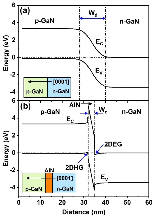
Fig. 1. Simulated energy band diagram of (a) a vertical p-n junction in
GaN (inset) and (b) p-n junction with AlN barrier (inset), where the
doping density in each n- or p- type region is
. The
polarization charge at the AlN/GaN interface helps reduce the
depletion width to facilitate tunneling.
In conventional tunneling devices, such as Zener diodes in
Si, degenerately doped regions located adjacently, achieve high
band bending that facilitates carrier tunneling through the
energy band gap. Fig. 1 (a) and the inset therein show the
simulated energy band diagrams for a degenerately doped
(
) p-n junction in GaN. The
depletion width at the junction in this case is more than ,
which greatly suppresses band to band tunneling of carriers on
either side. To overcome this, a thin layer of AlN is sandwiched
between p- and n- type regions (inset Fig. 1 (b)), which
introduces polarization charge at each of its interfaces with
GaN. This results in a high electric field across AlN
( [10]), thereby providing a sharp band bending
to enable band-to-band tunneling, as observed in Fig. 1 (b).
This mechanism has been utilized to implement tunnel diodes
and light emitting diodes [9]–[11].

Fig. 2. (a) Schematic of a
GaN Zener diode with a 2.8
nm AlN barrier layer sandwiched between p-GaN and n-GaN, (b)
Comparison of our simulation model with the reported experiment data
reported from [10] (Adapted from Fig. 3 (a) with permission from [10]
Copyright (2009) by the American Physical Society). The inset shows
the simulation results of on-current for different AlN thicknesses.
The tunneling rate via the non-local BBT model is
benchmarked by adjusting the effective electron tunnel mass
and hole tunnel mass
, using reported I-V data for a
GaN tunnel diode, a two-terminal device, with a
2.8 nm AlN barrier and and ohmic contacts for
p- and n- GaN, shown in Fig. 2 (a) from [10]. This device
showed a total specific resistivity (including the tunnel
resistance) of
. Effective masses
and
for GaN and
and
for AlN
[23], [32], produce simulated I-V results that closely follow
experimental characteristics, as shown in Fig. 2 (b), plotted for
different contact resistivity values of the p-GaN contact. A
good match between the model and experimental results is
achieved with a contact resistivity anywhere between
, which agrees with contact resistivities in the range
of
for [34], [35]. Since better
contacts to p-GaN, with
as low as
have been
realised with a proper choice of metal stack [36], we
optimistically employ
as the contact resistivity in
all the simulations of a three-terminal p-channel HTFET. With
this value of contact resistivity, the behaviour of the on-current
(current at of applied bias) at different thicknesses of AlN
is plotted in the inset in Fig. 2 (b). As seen, the device current
remains close to zero for AlN thickness less than or
greater than . This is because a thin AlN layer fails to
provide sufficient band bending required for the BBT, while a
thicker AlN increases the length of the tunnel barrier, resulting
in exponential degradation of the tunnelling current. The on-
current of the device peaks around of AlN thickness,
resulting in a minimum total specific resistivity of
.
III. NON-AMBIPOLAR OPERATION OF P-CHANNEL GAN
HTFET
Fig. 3 (a) shows a schematic diagram of the p-channel GaN
HTFET with its vertical direction along [0001]. From the
bottom to the top, the structure consists of a n-GaN
source, AlN tunneling barrier, undoped GaN (u-
GaN) channel and p-GaN. The energy of carriers in the
u-GaN channel is modulated by a Al
2
O
3
separated gate,
either in rectangular geometry with double gate or cylindrical
geometry with a gate-all-around architecture. Unless stated
otherwise, the width of the device in either rectangular or
cylindrical geometry is kept at , in-line with the
minimum reported GaN nanowire widths of 14 nm or 10 nm
reported via experiment in [37], [38]. As shown in the
corresponding band diagram in Fig. 3 (b), the u-GaN acts as
channel and maintains the valence band sufficiently lower than
both the hole quasi fermi level (
) as well as the
conduction band in the n-GaN, thus preventing the tunneling
of carriers when the gate bias is zero.
Fig. 3. (a) Schematic diagram of a p-channel GaN heterojunction
tunnel FET (HTFET), and its simulated band diagrams along
(b) at zero gate bias (OFF state), (c) negative gate bias (ON state) and
(d) positive gate bias (OFF state), and (e) transfer characteristics
showing non-ambipolar behaviour, similar to a p-channel MOSFET.
A negative gate bias, raises the energy of the bands in the
channel, moving the valence band closer to the hole quasi
fermi level (
), as shown in Fig. 3 (c), which leads to an
increase in hole concentration. At sufficiently large negative
gate bias, the valence band in the channel aligns with the
conduction band of n-GaN, hence enabling tunneling across the
AlN barrier, as indicated by the arrow in Fig. 3 (c) and turning
the device on. On the other hand, a positive gate bias reduces
the energy levels of the conduction and valence bands in the u-

GaN channel, as shown in Fig. 3 (d). However, since no AlN
layer is present at the interface between p-GaN and u-GaN, the
band bending between p-GaN and u-GaN occurs over a large
distance, which greatly suppresses the tunneling current to
maintain the device in the off-state.
The drain to source current
with respect to
for a
rectangular or fin geometry is plotted in Fig. 3 (e) for a device
or channel width of . In contrast to the n-channel GaN
HTFET reported in [14] where the channel is also doped,
utilisation of u-GaN as a channel layer reduces the leakage by
10 orders of magnitude. However, the bias requirement of this
device also increases to raise the energy of the valence band for
alignment with the conduction band across the AlN layer. A
lightly doped channel could also be employed to reduce the
operating bias of this device. As can be observed, the drain
current remains orders of magnitude lower at positive gate bias
than at negative gate bias, thus confirming non-ambipolar
behaviour, as indicated by the band diagrams (Fig. 3 (d)).
Owing to the wide band gap nature of GaN, the off-current of
the device remains much lower at
even for a
small channel length of . A large band gap of AlN
however, also introduces a large tunneling barrier height,
which makes it difficult for the charge carriers to tunnel across
the AlN. Hence the maximum drain current or on-current
remains limited to in a fin geometry.
IV. OPTIMISED CYLINDRICAL P-CHANNEL GAN HTFET
The most common technique to improve the on-current in
TFETs is to introduce a highly doped pocket of opposite
polarity in the vicinity of the source edge of the channel to
enhance the electric field across the tunneling junction [39],
[40]. Moreover, a better electrostatic gate control is expected
in cylindrical or nanowire geometry. Hence, in this section, we
analyse the electrical characteristics of an optimised cylindrical
GaN HTFET, which utilises a thin () and highly doped
(
) pocket at the interface between channel
and an AlN barrier of 1.7 nm thickness of GaN HTFET, as
shown in Fig. 4, while the rest of the dimensions are kept the
same as that for the device in Fig. 3 (a).
The electrical characteristics of the p-channel GaN HTFET
are presented in Figs. 4 (a) and 4 (b), respectively. The current
is normalised to the diameter of the cylindrical geometry.
Owing to the thin p-GaN pocket, the maximum drain on-
current
in Fig. 4 (a) is more than double in comparison to
a rectangular device without the pocket (Fig. 3 (e)). An
improved gate control in the cylindrical geometry also leads to
a much steeper subthreshold slope (SS) of , in the
absence of defect or trap states. In the absence of the thin AlN
layer at the top edge of the gate, a positive gate bias alone is
insufficient to produce a large band bending at this interface,
hence the device continues to remain non-ambipolar. In Fig. 4
(b), it can be noted that a higher
is required to turn-on the
device as
is increased. This is because a high
not
only raises the energy of the valence band in the channel but
also increases the energy of the conduction band in n-GaN
across the AlN barrier layer (Fig. 3 (c)), thus requiring a higher
to align the bands to turn the device on.
Fig. 4. Optimised (a)
and (b)
characteristics for
the cylindrical p-channel GaN HTFET with a 2 nm pocket and 1.7 nm
AlN barrier layer. (c) Impact of traps and trap-assisted tunneling
(TAT) on transfer characteristics.
The impact of traps with densities
and
in AlN and resulting trap-assisted tunneling
(TAT) is analysed in Fig. 4 (c). Owing to the higher
recombination, the maximum drain current of the device
degrades. Due to the increased leakage caused by TAT, the SS
of the device no longer remains below . Even
though the device turns on at a relatively smaller
, it