ISBN 978-80-261-0602-9, © University of West Bohemia, 2016
A Quadrature Modulator Based Scheme for
Frequency Hopping Applications
Burak Soker, Sinan Kurt, Gokhun Selcuk
HBT-ETM
ASELSAN Inc.
Ankara, Turkey
bsoker,sinank,gselcuk@aselsan.com.tr
Abstract – In this study a new frequency hopping scheme
which relies on digital up-conversion of baseband data is
proposed. Since the frequency of the local oscillator is
kept constant and hopping is achieved in the baseband,
the time required for the frequency jump is independent
of the frequency step, allowing a narrow loop bandwidth
and low noise performance for conventional phase
locked loops (PLLs). Moreover the spurious signals
resulting from the modulator is around -70 dBc, which
is a lower value when compared to spurious signal
performance of commercially available direct digital
synthesis (DDS) integrated circuits. We have analyzed
the error vector magnitude (EVM) and frequency
hopping speed on a practical setup and have shown that
quite satisfactory results can be obtained with the
proposed scheme.
Keywords -frequency hopping; digital up-conversion;
quadrature modulator; phase locked loop; direct digital
synthesis
I.
I
NTRODUCTION
Spread spectrum systems are widely utilized in
order to overcome performance degradation due to
jamming and interference arising from other users. In
frequency hopped spread spectrum (FHSS), the data is
organized into blocks and each block is transmitted
with a different pseudo random carrier frequency
enabling redundancy.
In FHSS, no data is transmitted until the carrier
frequency is tuned to the next destination frequency
which reduces the effective data rate of the whole
system. The carrier signal is generated either by using
a voltage controlled oscillator (VCO) whose tuning
voltage is adjusted within the phase locked loop (PLL)
or a direct digital frequency synthesizer (DDFS),
which generates the carrier signal with a digital to
analog converter (DAC) according to the frequency
tuning word.
In applications where conventional PLL’s are used,
the frequency hopping speed is primarily determined
by loop dynamics. The time required for a PLL to lock
to a target frequency is given by [1],
(
)
n
tol
lock
ff
t
ξω
ξ
/1ln
2
Δ−−
=
(1)
where
ξ
is the damping factor,
n
ω
is the closed loop
bandwidth,
fΔ
is the frequency step and
tol
f
is the
tolerance around the destination frequency. In order to
increase the settling speed, the loop bandwidth can be
increased but this will result in degradation in the
phase noise performance of the PLL affecting the
ultimate error vector magnitude (EVM) of the whole
system. Moreover, the settling time is a function of the
frequency step and in the design phase the maximum
frequency step should be used as one of the design
criteria. Although studies are conducted to alleviate
the difficulty regarding the settling time [2-4],
significant performance improvements could not be
obtained without an additional effort.
An alternative solution to conventional PLLs is to
generate the carrier signals digitally by using
commercially available DDFS integrated circuits. As
the carrier signal is digitally produced, the time
required for a frequency jump is limited by nothing
but the register writing speed, therefore DDFS is much
faster than the conventional PLL architecture [5].
However it has two main disadvantages. The first one
is that, the maximum frequency that a DDFS can
synthesize is limited upto only a few GHz, making
their use impractical for high frequency applications,
unless a hybrid approach, which includes the use of
PLL as well, is utilized. The other main drawback of
DDFS is that, digital generation of carrier signals
introduces spurious signals as strong as -50 dBc which
makes it difficult to satisfy spectrum mask
requirements [6].
In the present study, we propose a novel scheme
based on digital up-conversion of the baseband data,
which is used to modulate a quadrature modulator. As
the frequency hopping is performed at the baseband,
the maximum frequency jump is limited by the
sampling frequency of the DAC. Considering the
performance of the commercially available DACs, the
proposed method is suitable for systems with sub-GHz
frequency jumps. The local oscillator for the
modulator is supplied from a conventional PLL with
narrow loop bandwidth; hence there is no contribution
to EVM from the carrier signal. The carrier leakage
and the sideband suppression of the modulator can be
calibrated such that they are both lower than -70 dBc,
which is considered as an improvement over DDFS
systems.
We have tested the proposed scheme on a practical
setup and obtained satisfactory results in terms of
frequency hopping speed and EVM. The hopping
speeds on the order of nanoseconds and the EVM
values less than %1 are observed over the whole
bandwidth.

II.
T
HE
P
ROPOSED
S
CHEME
Block diagram of the proposed scheme, namely
digitally up-converted IQ data generation, is illustrated
in Fig. 1.
Figure 1. Generation of digitally up-converted data
As shown in Fig. 1, the frequency jump is achieved
using a full complex mixer and a numerical oscillator
(NO) at frequency ω
m
. The new in phase and
quadrature signals are generated according to,
() ()
ttQttItI
mdatamdatadata
ω
ω
sin)(cos)()( −=
′
(2a)
() ()
ttIttQtQ
mdatamdatadata
ω
ω
sin)(cos)()( −=
′
(2b)
where ω
m
is the frequency of the NO and the primed
data variables refer to the digitally up-converted data.
Despite the ideal multiplication as depicted in Fig.
1, some detrimental factors degrade the performance
of this system. Since IQ signals are up-converted in
the baseband before conventional mixing, the DAC
can not be operated at the same frequency as if there is
no up-conversion. Not only the bandwidth but also the
frequency shift of the IQ data should be considered
while selecting the minimum sampling frequency of
the DAC. The DAC sampling frequency can be
written as,
()
Wff
s
+Δ⋅> 2
(3)
where
s
f
is the sampling frequency,
fΔ±
is the
maximum frequency jump and W is the bandwidth of
the signal. Note that, the generated baseband signal
has a bandwidth W, before frequency shift. Therefore,
in this equation W is used as the one-sided bandwidth.
Use of high frequency DACs instead of their low
frequency counterparts is undesirable when power
consumption, noise performance and harmonic
distortion parameters are considered. Due to the
necessity of the use of a high speed DAC, the phase
noise performance at the output of the modulator will
be determined by the NO. High quantization noise of
the DAC will dominate the total phase noise of the
modulator. It should be noted that the sampling
frequency limited by (3), is much less than the
sampling frequency of the DACs employed in DDS
circuits. Therefore the method proposed in this study
will lead to improved results in terms of phase noise
performance and harmonic distortion when compared
to systems employing DDS in their architectures.
Apart from the degradations introduced by high
speed DACs, some spurious content is also introduced
by the imbalance of the quadrature modulator. The
phase/amplitude imbalance between the in-phase and
quadrature paths will result in some carrier leakage
and sideband signals to be observed at the output
spectrum of the modulator. Given the phase imbalance
θ
in degrees and the amplitude imbalance
α
in dB,
the sideband signal level (SSL) in dBc’s is given by
[7],
()
2/cotlog20
..
θ
=
imbphase
SSL (4)
+
−
=
110
110
log20
20/
20/
..
α
α
imbamp
SSL
(5)
Since the frequency of the transmitted data and the
local oscillator signal do coincide, these spurious
signals in (4,5) will appear outside the bandwidth
allocated for the channel, possibly violating spectrum
mask requirements. Moreover as the frequency of the
I/Q signals is increased, the system is less immune to
differences due to path difference between the
transmission line paths of I/Q signals. Also the
specifications of both I/Q modulator ICs and DACs
degrade at high speeds, deteriorating spur
performance. Although the IQ imbalance may seem a
serious problem for the proposed scheme, it should be
noted that the detrimental effects due to the imbalance
can be compensated by proper calibration of the
phase/amplitude of the baseband signals. Undesired
spurious signals can be decreased to about -70 dBc,
which is a satisfactory value when compared to
spurious performance of commercially available DDS
components.
III. P
RACTICAL
I
MPLEMENTATION
In order to test the performance of the proposed
scheme, we used a practical setup whose block
diagram is shown in Fig. 2.
Figure 2. Block diagram of the setup.
The digitally generated data is fed to 100 Mbps 16-
bit DACs internal to E4438C signal generator. The
outputs of the DACs are filtered using a 40 MHz low-
pass filter to eliminate aliasing terms from the DAC.
The filtered baseband signal is fed to the quadrature
modulator. The quadrature modular used in the setup
is BGX7101 from NXP which supports wide
modulation bandwidth (650 MHz). The local oscillator
for the modulator is supplied from another signal
generator with low phase noise.

The phase noise at the output of the modulator is
determined by both the PLL and the DAC. In order to
test the phase noise performance of the scheme we
generated unmodulated signals at different offsets
from the PLL frequency. The phase noise
measurements are plotted in Fig. 3.
Figure 3. Phase noise at the output of the modulator
The blue curve in Fig. 3 plots the phase noise
performance of the PLL which is operated at 2.5 GHz.
As for the green and black curve measurements, IQ
modulator output is digitally shifted 1MHz and
25MHz respectively. Therefore, using the same PLL
frequency, namely 2.5GHz, the green and black curves
show the phase noise performance at the frequencies
2.501 GHz and 2.525 GHz. Since green and black
curves result in similar phase noise plots, we conclude
that the clock phase noise of the DAC is negligible and
the main contributors are the quantization noise and
thermal noise of DAC.
Next we observed the spurious performance of the
proposed scheme. In Fig. 4 the output spectrum of the
IQ modulator is plotted with LO frequency adjusted to
2.5 GHz. The baseband signals are generated such that
a sine wave at frequency 2.525 GHz is observed at the
output of the modulator.
Figure 4. Spur performance of the modulator.
In Fig 4 two types of spurious signals are observed.
The spurs at 2.5 GHz and 2.475 GHz are the carrier
feed through and the sideband signals due to the
imbalance of the baseband data. These spurs have the
amplitudes of -76.14 dBc and -70.4 dBc respectively.
The spurious signal at 2.45 GHz results from the
nonlinearity of the DAC and is 76.57 dB below the
carrier. Due to the low-speed operation of the DAC, its
spurious free dynamic range is higher. Therefore the
main contributor to the spurious performance in this
scheme is signals arising from the modulator
imperfections. It should be noted that the spurious
performance of this scheme is about 70 dBc, which
can be considered as a quite satisfactory result
outperforming commercially available DDS-ICs
operating at GHz frequencies.
In order to investigate the detrimental effects due
to the digital up conversion, we have also generated a
QPSK signal. The baseband signal is up-converted
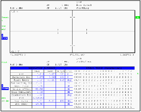
above 25 MHz of the carrier frequency. EVM is
measured about 0.3%, which is the lower limit of the
measuring device. It can be deduced that the digital
up-conversion does not deteriorate the EVM
performance. The constellation diagram and the
measured values are given in Fig. 5.
Figure 5. The constellation diagram for the QPSK signal
Figure 6. Frequency transition in the proposed scheme
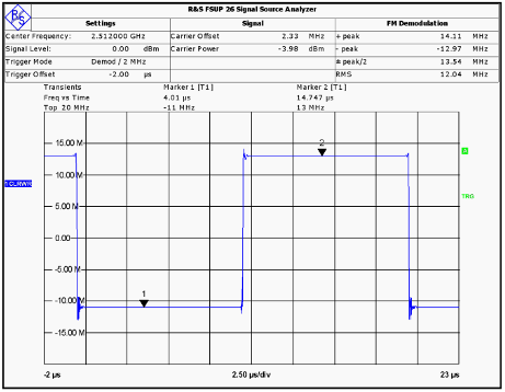
Finally we investigated the frequency settling time
of the scheme by sequentially generating two
baseband signals leading to different carrier
frequencies at the output of the modulator. The

frequency jump from 2.525 GHz to 2.501 GHz is
shown in Fig. 6.
The fluctuations seen at the edges of the frequency
transitions in Fig. 6 are due to the glitches generated
by the DAC. These glitches are filtered by the 30 MHz
bandwidth of the measuring device. Due to the limited
bandwidth of the measuring device, the settling time
could not be obtained accurately. However we can
deduce that the settling time is on the order of a few
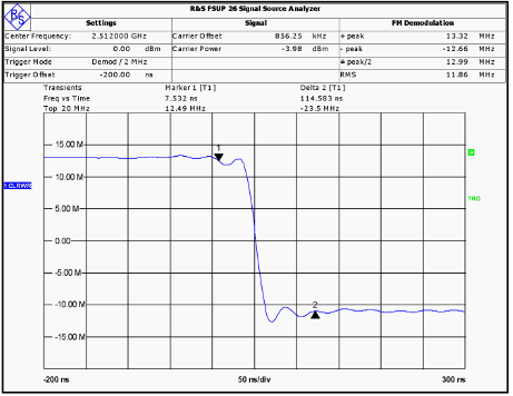
hundred nanoseconds. The detailed frequency
transition plot is given in Fig. 7.
Figure 7. Frequency transition enlarged
IV. C
ONCLUSIONS
In this study, we propose a novel method to
generate frequency hopping signals using a quadrature
modulator. Instead of hopping the carrier frequency of
the quadrature modulator, frequency change is
achieved by digital up-conversion of the baseband
data. Using this method, the requirement of the DAC
specifications is considerably reduced as compared to
the DACs employed in DDS circuits. This is because
the maximum speed of the DACs is determined by not
maximum operating frequency but maximum offset
needed for the frequency hop. Because of the low-
frequency operation of the DAC in the proposed
scheme, both quantization noise and SFDR are
improved leading to lower phase noise and better
dynamic range. Moreover the settling time, which is
constrained by the loop dynamics of the PLLs, is no
more of concern. In the proposed scheme, the
frequency hop can be achieved instantly as in the case
of DDS-ICs. Furthermore, spurious levels are not
limited by DAC performance but rather modulator
spurs and can be decreased severely by proper
calibration of the baseband IQ signals. The spur levels
measured in the proposed scheme are lower compared
to the high-speed DACs within DDS-ICs.
R
EFERENCES
[1] A. Cicero, Architectures for RF Frequency Synthesizers,
Kluwer Acad. Pub., New York, US, 2003.
[2] X. F. Kuang and N. J. Wu, “A fast-settling monolithic PLL
frequency synthesizer with direct frequency presetting,” in
ISSCC Dig. Tech. Papers, pp. 204–205, pp. 855-865, Feb.
2006,.
[3] A. Zhang, P. E. Allen, J. M. Huard, “ A fast switching PLL
frequency synthesizer with an on-chip passive discrete-time
loop filter in 0.25 um CMOS,” IEEE J. Solid-State Circuits,
vol.38, no. 6, Jun. 2003
[4] K. Woo, Y.liu, E.Nam and D. Ham, “Fast-lock hybrid PLL
combining fractional-N and integer-N modes of differing
bandwidths,” IEEE J. Solid-State Circuits, vol. 43, no. 2, pp.
379-389, Feb. 2008
[5] J. Vankka, “Digital frequency synthesizer/modulator for
continious-phase modulations for slow frequency hopping,”
in IEEE Trans .on Veh. Tech. , vol.38, pp. 933-940, no. 4,
Nov. 1997
[6] K. Kwon, W. Yoon, “ Methods to supress DDFS spurious
signals in a frequency-hopping synthesizer with DDFS-driven
PLL architecture,” in IEEE Trans. on Ultr Ferro. Freq. Cont. ,
vol.57, pp. 299-304, no. 2, Feb. 2010
[7] C. L. Liu, “Impacts of I/Q imbalance on QPSK-OFDM-QAM
detection”, IEEE Trans. Cons. Electr., vol. 44, no 3, pp 984-
989, Aug. 1998


