Turk J Elec Eng & Comp Sci
(2019) 27: 3114 – 3137
© TÜBİTAK
doi:10.3906/elk-1811-168
Turkish Journal of Electrical Engineering & Computer Sciences
http://journals.tubitak.gov.tr/elektrik/
Research Article
A quasi-Z-source active neutral point clamped inverter topology employing
symmetrical/unsymmetrical boost modulation control scheme for renewable
energy resources
Rehan MAJEED
1,2,∗
,, Danial SALEEM
2
, M. Imtiaz HUSSAIN
3
,, Muhammad Talha GUL
4
,,
Muhammad Rehan USMAN
1
,, Salman MAJEED
1
1
Department of Electrical Engineering, Superior University, Lahore, Pakistan
2
Department of Protection and Control, National Transmission and Despatch Company, Lahore, Pakistan
3
Green Energy Technology Research Center, Kongju National University, Cheonan, South Korea
4
Department of Electrical Engineering, Sharif College of Engineering, Lahore, Pakistan
Received: 26.11.2018 • Accepted/Published Online: 29.03.2019 • Final Version: 26.07.2019
Abstract: This paper proposes a bipolar quasi-Z-source active neutral point clamped inverter (QZS-ANPCI) topology.
It acts as a buck/boost inverter (3-phase, 3-level) to integrate renewable energy resources under their uctuating
DC voltages. We propose a symmetrical/unsymmetrical boost modulation control technique to mitigate the DC-link
unbalance voltage problem in an ANPC inverter. This worthwhile control technique exploits voltage-current closed-
loops on AC and DC sides to regulate the desired parameters. Moreover, the constant boost control (CBC) modulation
has provided a switching sequence that generates a symmetrical/unsymmetrical full shoot-through (FST) state for
boosting input DC voltage in the proposed inverter. Detailed loss and eciency analysis is carried out to show its
superior performance under the proposed scheme. Furthermore, the total harmonic distortion (THD) of the proposed
QZS-ANPCI meets IEEE Standard-519. Simulink/MATLAB (MathWorks, USA) and PSIM (Powersim, USA) software
programs are used to simulate the proposed topology. To verify the theoretical proposals and simulation results, we have
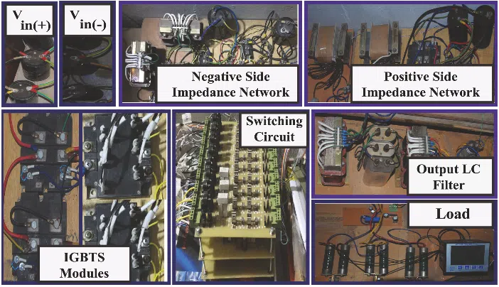
developed an experimental prototype setup (1 kW). Both simulation results and experimental data show satisfactory
agreement and support the theoretical postulates.
Key words: Z-source inverter, quasi-z-source inverter, buck/boost inverter, neutral point clamped inverter, active
neutral point clamped inverter
1. Introduction
Renewable energy resources (RERs) are penetrating into electrical power systems. This trend is due to the rising
inevitable problems of global warming. The main reason is the excessive consumption of fossil fuel for energy
generation. Over the years, several RERs such as solar, wind, hybrid solar-gas, and biomass resources have been
explored and developed for alternative power generation [1]. Power conditioning converters are mandatory to
interface RERs with utility grid systems. Therefore, the voltage-fed inverter (VFI) and the current-fed inverter
(CFI) are two main conventional power inverters that synchronize these resources with interconnected utility
grids. These converters do not have the boost ability during low DC input voltage. Instead, they require separate
DC-DC boost converters at their input stage. The Z-source inverter (ZSI) [2], developed in 2003, has a built-in
buck/boost characteristic to overcome the above problems. The ZSI exploits unipolar X-shaped impedance (Z)
∗
Correspondence: rehan_majeed2008@yahoo.com
This work is licensed under a Creative Commons Attribution 4.0 International License.
3114

MAJEED et al./Turk J Elec Eng & Comp Sci
integrated with the conventional inverter. It contains capacitors (C) and inductors (L) as passive components.
Due to its inherent characteristics, classical converters, such as DC-DC, AC-DC, DC-AC, and AC-AC, can have
buck/boost ability working together with the same impedance [3].
An improved form of the ZSI is the QZSI to overcome its problems. There are four distinct QZSI
topologies for RERs. These topologies have various advantages, such as a continuous input current, lower
component ratings, reduced component count, reduced input source stress, and simplied control strategies
compared to the conventional ZSI [4]. There are many pulse-width modulation (PWM) techniques for ZSIs.
These techniques include simple boost control (SBC), maximum boost control (MBC), constant boost control
(CBC), and developed space-vector pulse width modulation (SVPWM) control. The conventional ZSI topologies
have employed modulations in dierent research works [5, 6].
The most popular multilevel inverter developed to overcome the limitations of VFIs is the neutral point
clamped inverter (NPCI). This is because it has lower voltage stresses, switching losses, conduction losses,
switching frequency, and THD than those of 2-level inverters [7, 8]. Therefore, it has many applications at
medium voltage levels. Furthermore, the authors of [9] applied the z-source impedance concept in NPCI. Also,
the works in [10, 11] derived a Z-source NPCI structure to decrease the number of passive components and also
proposed a modulation scheme. Due to improved performance of the quasi-Z-source impedance, the works in
[12, 13] presented a proposed single-phase quasi-Z-source NPCI and its modulation scheme. To overcome the
drawbacks of the traditional Z-source NPCI, the work in [14] also presented two transformer-based z-source
NPCI structures. Recently, Yu [15] demonstrated a simulation-based proposed quasi-Z-source NPCI topology
with reduced capacitor voltage. Another research study in [16] proposed an LC-switched NPCI topology to
reduce the number of passive components. This topology multilevel inverter uses a symmetrical boosting control
method (FST).
Furthermore, the authors of [17] proposed a 3-level boost PFC converter and control scheme to improve
voltage imbalance and zero current distortion. They can feed to linear loads as well as nonlinear loads
nonsymmetrically. The authors of [18] developed a PFC rectier-based multilevel boost converter using a
nonsymmetrical active capacitive divider structure. This structure reduces the switching losses and uses a
smaller inductor. Also, 4-level operation is achieved instead of 3-level converter operation with the same number
of components . Another research study implemented a single voltage source-based DC-link capacitors voltage
balancing technique for NPC inverters using an inductor boost topology [19]. This used a single source-based
simple DC-DC boost stage at the NPCI input.
Recent studies have explored new multilevel boost topologies and control strategies to provide improved
performance. The work in [20] developed a single-phase modied quasi-Z-source cascaded hybrid inverter (5-
level). This uses a greater number of components and uses only a symmetrical boosting technique for a single
input source. This is a cascaded topology with a greater number of components. Moreover, a dual-T-type
seven-level boost ANPC topology, proposed in [21], provides a scheme for balancing the voltage of oating
capacitors (FCs). This scheme feeds to a 3-phase load using a single input source. This converter topology is
two-staged dual T-type and increases the complexity.
For recent control techniques, the work in [22] proposed a PWM strategy for a cascaded H-bridge inverter
to cope with unbalanced DC input sources. This study does not have a voltage boosting stage in cascaded
topology. In the same way, the SVPWM technique proposed in [23] can balance neutral point voltage in a
low voltage T-type NPC inverter. It generates nonsymmetrical shoot-through states to deal with input voltage
3115

MAJEED et al./Turk J Elec Eng & Comp Sci
variations. Similarly, the carrier-based PWM technique was developed for two separate PV MPPTs supplying
power to a T-type inverter (3-level) [24].
However, this paper focuses on two independent input voltage sources (positive and negative sides) instead
of a single input voltage source. These sources may be RERs with large variations of voltages independently.
This study also proposes a symmetrical/unsymmetrical boost control technique for independent RERs using
modied CBC-PWM to provide balanced DC-link voltages. This mitigates the problem of unbalancing DC and
AC voltages and improves the performance of converter, whereas the conventional Z-source NPC or multilevel
inverter oers the feature of symmetrical boosting control method (FST). They are usually designed to feed
the 3-phase balanced loads if input voltages sources are equal and identical, but if positive and negative side
input voltages are independent RERs and their magnitude uctuates then they suer from unbalancing output
voltage, increased THDs, and neutral point shifting issues. They require an unsymmetrical boost control method
to overcome these issues.
In this paper, we have contributed to the literature in the following ways. First, we have proposed a
QZS-ANPCI topology. Since the multilevel ANPCI has superior performance as compared to multilevel NPCI
[17, 18], a 3-level ANPCI topology has been combined with a dual quasi-Z-source impedance network. We have
developed a modulation control scheme to provide its ecient performance. To evaluate the results, we have
performed a simulation of the proposed system in Simulink/MATLAB and PSIM softwares. Finally, we have
veried these results by developing a hardware prototype model.
The structure of this article is as follows: Section 1 has described the background history of ZSI topology.
Section 2 presents the theoretical development of the control scheme. Section 3 provides a detailed theoretical
and mathematical analysis of the proposed topology. Section 4 presents the simulation results. Section 5
illustrates experimental results and discussion. Section 6 evaluates the conclusion.
2. Proposed control strategy and modulation technique
Previously, the authors of [6] proposed a constant boost control (CBC) modulation as depicted in Figure 1a.
It has better performance as compared to other PWM modulation techniques. Moreover, this technique has
increased modulation index M , from 1 to 2/
√
3. The reference voltages (Va, Vb, Vc) are mixed with a third
harmonic component having 1/6 the magnitude of the fundamental component to form CBC modulation signals.
When carrier signals exceed two straight lines ( V
P
, V
N
), then uniform upper and lower ST pulses are generated.
The upper and lower side ST pulses turn on the inverter leg switches (G
1X
, G
2X
, G
3X
, X = {1, 2, 3, 4})
simultaneously in the traditional FST state for a short period of time. However, in the proposed modulation
technique, upper side inverter switches (G
1X
, G
2X
, G
3X
, G
Y 5
, X = {1, 2}, Y = {1, 2, 3}) undergo the on-state
simultaneously to produce the upper side ST state. The lower side switches (G
1X
, G
2X
, G
3X
, G
Y 6
, X =
{3, 4}, Y = {1, 2, 3}) conduct to generate the lower side ST state. These pulses have upper and lower side
ST duty ratios (D
0P
, D
0N
) to boost input DC voltages. If the upper side ST duty ratio (D
0P
) is equal to
the lower side ST duty ratio (D
0N
), then FST and full nonshoot-through (FNST) states are generated [11].
This type of traditional voltage boost is known as symmetrical boost conversion. The single carrier-based CBC
generates ST states with a frequency two times the carrier frequency. However, bipolar carrier-based CBC
produces the same ST states at the frequency as that of carriers.
If upper and lower ST duty ratios (D
0P
, D
0N
) have dierent values, then rst FST occurs and next
either the upper or lower ST state occurs in a switching cycle as illustrated in Figure 1b. The modulation
3116

MAJEED et al./Turk J Elec Eng & Comp Sci
scheme calculates the modulation index M taking the highest ST duty ratio that is the greater value among
D
0P
and D
0N
. Therefore, this type of proposed voltage boost is called unsymmetrical boost conversion. The
proposed modulation technique can perform both symmetrical and unsymmetrical boost conversion. These ST
states are inserted into zero states of traditional inverter. This type of modulation does not distort AC side
power ow. The ST duty ratio (D ) is expressed by Eq. (1).
D =
1 −
√
3M
2
(1)
0
1
-1
LST
UST
G
G
G
G
1
2
3
4
V
a
0
1
0
1
0
1
0
1
0
1
0
1
0.02 0.022 0.024 0.026 0.028 0.03 0.032 0.034 0.036 0.038 0.04
V
a
V
b
V
c
0.03
0.0305
0.031 0.0315 0.032
T ime (s)
V
p
V
N
Carier 1
Carier 2
V
m
0
1
-1
V
abc
(a) Traditional constant boost control (CBC) using sym-
metrical boost modulation scheme
V
0.03
0.0305
0.031 0.0315 0.032
T ime (s)
0.02 0.022 0.024 0.026 0.028 0.03 0.032 0.034 0.036 0.038 0.04
0
1
-1
LST
UST
G
G
G
G
1
2
3
4
V
a
0
1
0
1
0
1
0
1
0
1
0
1
V
a
V
b
V
c
V
p
V
N
Carier 1
Carier 2
V
m
0
1
-1
abc
(b) Proposed constant boost control (CBC) using unsym-
metrical boost modulation scheme
Figure 1. Traditional and proposed modulation schemes.
3. Proposed quasi-Z-source ANPC inverter (QZS-ANPCI) topology
Here we present the proposed QZS-ANPCI topology and its detailed control scheme for RERs, as illustrated in
Figures 2a and 2b. The operating principle is equivalent to that of a conventional buck/boost Z-source NPC
inverter [11]. In this proposed topology, there are four switching modes of operation over one switching time
period (T ). These modes repeat the ST and NST states two times in a switching sequence.
Moreover, we propose the proportional integrator (PI) regulator, proportional (P) regulator, and control
scheme according to [19, 20]. There are two DC-side voltage-current closed-loop controllers. Here, the DC-link
voltages (V
P N
*, V
NN
*) used in each outer loop with the PI regulator are reference constant voltages. The
feedback DC-link voltages (V
P N
, V
NN
) are compared with the reference DC-link voltages. An output of the
3117

MAJEED et al./Turk J Elec Eng & Comp Sci
Figure 2. Detailed schematic of proposed QZS-ANPCI and its control scheme: (a) proposed topology and its control
scheme, (b) internal detailed controller block of proposed SPWM with CBC technique.
outer loop PI regulator ensures tracking of the desired DC-link voltage. However, the feedback inductor currents
(I
L1
, I
L3
) used in the inner loop with the P regulator rapidly improve the dynamic response. These controllers
generate the upper and lower side ST signals to boost the input DC voltages.
In the same way, there is one AC-side voltage-current closed-loop controller in the control scheme. The
output RMS voltage (V
abc
*), used as a reference voltage, is compared with the feedback AC voltage (V
abc
). The
purpose of the outer loop PI regulator is to track the desired AC voltage under load current variation. While
3118