Correlation between morphology and ambipolar transport in organic field-effect transistors
TL;DR: In this paper, an approach to obtain ambipolar OFET with an active layer of organic semiconductor blends using semiconducting polymers in composite with fullerene derivatives is presented. But the results of this approach are limited.
Abstract: Attaining ambipolar charge transport in organic field-effect transistors (OFET) is highly desirable from both fundamental understanding and application points of view. We present the results of an approach to obtain ambipolar OFET with an active layer of organic semiconductor blends using semiconducting polymers in composite with fullerene derivatives. Clear features of forming the super position of both hole and electron-enhanced channels for an applied gate field are observed. The present studies suggest a strong correlation of thin-film nanomorphology and ambipolar transport in field-effect devices.
Figures (5)
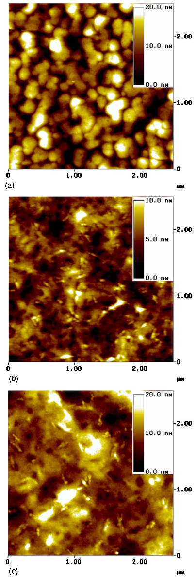
FIG. 4. sColor onlined The tapping mode AFM picture of MDMOPPV:PF:PCBMs1:1:2d blend on sad PVA, sbd BCB, and scd PVP which indicates large phase separated film on PVAsca. 200 nmd and less phase separated film on BCB and PVP. 
FIG. 3. sColor onlined Tapping mode AFM picture ofsad PVA, sbd BCB, and scd PVP. All the films have smooth surfaces with a height scale of 5 nm. 
FIG. 5. Typical transistor characteristics of unipolar OFET with MDMO– PPV:PF:PCBMs1:1:2d blend film coated on PVA dielectric. Inset: chemical structure of PVA. 
FIG. 6. sad Typical transistor characteristics of ambipolar OFET with MDMO–PPV:PF:PCBMs1:1:2d blend film coated on BCB dielectric with hole current with pinchoff occurring atVgs above −30 V and electron current with a well-defined pinchoff atVgs above +30 V.sbd Transfer characteristics of the ambipolar OFET with hole enhancement mode and electron enhancement mode demonstrating the clear superposition of both hole- and electron-enhanced channel formation for an appliedVgs. The arrows indicate the direction sweeping ofVgs. Inset: chemical structure of BCB. 
FIG. 7. Typical transistor characteristics of ambipolar OFET with MDMO– PPV:PF:PCBMs1:1:2d blend film coated on PVP dielectric demonstrating both hole enhancement mode and electron enhancement mode. Inset: chemical structure of PVP.


Citations
More filters
2,020 citations
TL;DR: Comparison of the optical properties of solution and thin film of thioxophospholes shows that these compounds do not form aggregates in the solid state, and variation of the substitution pattern of phospholes and chemical modification of their P atoms afford thermally stable derivatives, which are photo- and electroluminescent.
Abstract: The photophysical, electrochemical, and optoelectronic properties of conjugated systems incorporating dibenzophosphole or phosphole moieties are described. Dibenzophosphole derivatives are not suitable materials for OLEDs due to their weak photoluminescence (PL) in the solid state and the instability of the devices. Variation of the substitution pattern of phospholes and chemical modification of their P atoms afford thermally stable derivatives, which are photo- and electroluminescent. Comparison of the optical properties of solution and thin film of thioxophospholes shows that these compounds do not form aggregates in the solid state. This property, which is also supported by an X-ray diffraction study of three novel derivatives, results in an enhancement of the fluorescence quantum yields in the solid state. In contrast, (phosphole)gold(I) complexes exhibit a broad emission in thin film, which is due to the formation of aggregates. Single- and multilayer OLEDs using these P derivatives as the emissive layer have been fabricated. The emission color of these devices and their performances vary with the nature of the P material. Interestingly, di(2-thienyl)thiooxophosphole is an efficient host for the red dopant DCJTB, and devices using the gold complexes have broad emission spectra.
237 citations
TL;DR: The latest advances in the use of solution processable organic semiconductor blends for organic field effect transistor (OFET) applications are reviewed in this article, where multi-component, thin film microstructure formation from solution with particular focus on phase separation and crystallisation of components.
Abstract: The latest advances in the use of solution processable organic semiconductor blends for organic field effect transistor (OFET) applications are reviewed. We summarise multi-component, thin film microstructure formation from solution with particular focus on phase separation and crystallisation of components. These approaches can then be applied to semiconducting materials and their use in organic devices. Several key applications are studied, namely ambipolar systems with n- and p-type components, high charge carrier mobility and uniform films for high performance OFETs, and the potential for self-assembly during OFET fabrication. Blending materials can in all cases be used to combine the advantageous properties of the individual components.
225 citations
TL;DR: In this article, the authors deal with the use of solution processing approaches for organic electronics with a focus on material ink formulations as well as their applicability, including gravure printing, screen printing, and ink-jet printing.
Abstract: This review deals with the use of solution processing approaches for organic electronics with a focus on material ink formulations as well as on their applicability. The solution processing techniques include methods like gravure printing, screen printing and ink-jet printing. Basic principles of each approach are understood and fundamental correlations between material (metals, semiconductors, and dielectrics) ink properties and final device performances can be drawn. Nevertheless, solution processing methods have the potential to evolve as the most promising tools in organic device fabrication techniques and have already been applied successfully in the fields of organic thin film transistors, solar cells and biosensing devices.
180 citations
References
More filters
TL;DR: In this article, a spin-coated polymer gate dielectric layer was used to obtain a polyvinylphenol-based copolymer-based transistor with a carrier mobility as large as 3 cm2/V's and sub-threshold swing as low as 0.5 V/decade.
Abstract: We have fabricated pentacene organic thin film transistors with spin-coated polymer gate dielectric layers, including cross-linked polyvinylphenol and a polyvinylphenol-based copolymer, and obtained devices with excellent electrical characteristics, including carrier mobility as large as 3 cm2/V s, subthreshold swing as low as 1.2 V/decade, and on/off current ratio of 105. For comparison, we have also fabricated pentacene transistors using thermally grown silicon dioxide as the gate dielectric and obtained carrier mobilities as large as 1 cm2/V s and subthreshold swing as low as 0.5 V/decade.
1,225 citations
TL;DR: The sophistication and flexibility of the patterning procedures, high level of integration on plastic substrates, large area coverage, and good performance of the transistors are all important features of this work.
Abstract: Electronic systems that use rugged lightweight plastics potentially offer attractive characteristics (low-cost processing, mechanical flexibility, large area coverage, etc.) that are not easily achieved with established silicon technologies. This paper summarizes work that demonstrates many of these characteristics in a realistic system: organic active matrix backplane circuits (256 transistors) for large ( approximately 5 x 5-inch) mechanically flexible sheets of electronic paper, an emerging type of display. The success of this effort relies on new or improved processing techniques and materials for plastic electronics, including methods for (i) rubber stamping (microcontact printing) high-resolution ( approximately 1 microm) circuits with low levels of defects and good registration over large areas, (ii) achieving low leakage with thin dielectrics deposited onto surfaces with relief, (iii) constructing high-performance organic transistors with bottom contact geometries, (iv) encapsulating these transistors, (v) depositing, in a repeatable way, organic semiconductors with uniform electrical characteristics over large areas, and (vi) low-temperature ( approximately 100 degrees C) annealing to increase the on/off ratios of the transistors and to improve the uniformity of their characteristics. The sophistication and flexibility of the patterning procedures, high level of integration on plastic substrates, large area coverage, and good performance of the transistors are all important features of this work. We successfully integrate these circuits with microencapsulated electrophoretic "inks" to form sheets of electronic paper.
1,138 citations
TL;DR: In this article, the authors demonstrate that hole transport and electron transport are both generic properties of organic semiconductors and combine the organic ambipolar transistors into functional CMOS-like inverters.
Abstract: There is ample evidence that organic field-effect transistors have reached a stage where they can be industrialized, analogous to standard metal oxide semiconductor (MOS) transistors. Monocrystalline silicon technology is largely based on complementary MOS (CMOS) structures that use both n-type and p-type transistor channels. This complementary technology has enabled the construction of digital circuits, which operate with a high robustness, low power dissipation and a good noise margin. For the design of efficient organic integrated circuits, there is an urgent need for complementary technology, where both n-type and p-type transistor operation is realized in a single layer, while maintaining the attractiveness of easy solution processing. We demonstrate, by using solution-processed field-effect transistors, that hole transport and electron transport are both generic properties of organic semiconductors. This ambipolar transport is observed in polymers based on interpenetrating networks as well as in narrow bandgap organic semiconductors. We combine the organic ambipolar transistors into functional CMOS-like inverters.
806 citations
TL;DR: In this article, the authors have fabricated organic thin-film transistor (OTFT)-driven active matrix liquid crystal displays on flexible polymeric substrates using a low-temperature process.
Abstract: We have fabricated organic thin-film transistor (OTFT)-driven active matrix liquid crystal displays on flexible polymeric substrates. These small displays have 16×16 pixel polymer-dispersed liquid crystal arrays addressed by pentacene active layer OTFTs. The displays were fabricated using a low-temperature process (<110 °C) on flexible polyethylene naphthalate film and are operated as reflective active matrix displays.
792 citations
TL;DR: In this paper, a Pentacene-based thin-film integrated circuit with polymeric shadow masks and powered by near-field coupling at radio frequencies of 125 kHz and above 6 MHz has been demonstrated.
Abstract: Pentacene-based thin-film integrated circuits patterned only with polymeric shadow masks and powered by near-field coupling at radio frequencies of 125 kHz and above 6 MHz have been demonstrated. Sufficient amplitude modulation of the rf field was obtained to externally detect a clock signal generated by the integrated circuit. The circuits operate without the use of a diode rectification stage. This demonstration provides the basis for more sophisticated low-cost rf transponder circuitry using organic semiconductors.
753 citations