scispace - formally typeset
Search or ask a question
Journal ArticleDOI

Design, manufacturing, and performance analysis of mid-infrared achromatic half-wave plates with diamond subwavelength gratings

20 Aug 2012-Applied Optics (Optical Society of America)-Vol. 51, Iss: 24, pp 5897-5902
TL;DR: This analysis shows that diamond, besides its outstanding physical and mechanical properties, is a suitable substrate to manufacture mid-infrared HWPs, thanks to its high refractive index, which allows etching SWGs with lower aspect ratio.
Abstract: In this paper, we present a solution for creating robust monolithic achromatic half-wave plates (HWPs) for the infrared, based on the form birefringence of subwavelength gratings (SWGs) made out of diamond. We use the rigorous coupled wave analysis to design the gratings. Our analysis shows that diamond, besides its outstanding physical and mechanical properties, is a suitable substrate to manufacture mid-infrared HWPs, thanks to its high refractive index, which allows etching SWGs with lower aspect ratio. Based on our optimized design, we manufactured a diamond HWP for the 11-13.2 μm region, with an estimated mean retardance ~3.143±0.061 rad (180.08±3.51°). In addition, an antireflective grating was etched on the backside of the wave plate, allowing a total transmittance between 89% and 95% over the band.

Summary (3 min read)

1. Introduction

  • Wave plates are essential tools for modulating the polarization of an incoming light beam.
  • They are commonly used in many applications as retarders or phase shifters.
  • In astrophysics, when it comes to observing a very high-contrast scene, one must be able to cancel the bright source, or at least drastically reduce its intensity.
  • This attenuation can be achieved by combining two portions of the incident light beam, one of which having to undergo a half wavelength (or π) phase shift.
  • Therefore, a half-wave plate (HWP) is by definition the ideal tool.

2. Achromatic Half-wave Plates (HWPs)

  • Many new optical devices have been made with SWGs, such as high-efficiency diffraction gratings, polarization-selective gratings, wave plates, and monolithic antireflective structures [11] .
  • SWGs are micro-optical structures with a period Λ smaller than λ ∕ n, λ being the observed wavelength of the incident light and n the refractive index of the grating substrate.
  • Such structures do not diffract light as a classical spectroscopic grating does.
  • Instead, only zeroth transmitted and reflected orders are allowed to propagate outside the grating, and the incident wavefront is not affected by further aberrations.
  • The condition for having an SWG is defined by the grating equation, which determines whether a diffraction order propagates or not through the grating, EQUATION ) where θ is the incidence angle and n I and n II are the refractive indices of the incident and transmitting media, respectively.

B. Rigorous Coupled Wave Analysis (RCWA)

  • Common scalar theories of diffraction in gratings do not work in the subwavelength domain.
  • In order to simulate the grating response and to calculate its form birefringence, the authors must consider the vectorial nature of light.
  • For this purpose, the authors have performed numerical simulations using the RCWA.
  • The algorithm converts the grating-diffraction problem into a matrix problem, and solves the Maxwell equations from layer to layer.
  • The solution corresponds to the reflection and transmission matrices in the two modes (TE/TM), describing the entire diffractive characteristics of the simulated structure: the diffraction efficiencies (η m TE ) and (η m TM ), and the phase shift (ΔΦ TE-TM ).

3. Choosing an Appropriate Material: Diamond

  • For an HWP to keep its efficiency over a wide spectral band, the component must be optimized in order to minimize the phase shift error with respect to π: EQUATION.
  • Since the error is a function of the wavelength, the authors minimize the root mean squared (RMS) error ε rms over the entire spectral band.
  • The authors have performed RCWA simulations to optimize the grating parameters for a refractive index ranging from 1.5 to 2.8, and for several specific mid-IR spectral bands, corresponding to the transmission windows of the Earth atmosphere: L (3.5-4.1 μm), M (4.5-5.1 μm), and N (8-13 μm).
  • Other solutions beyond 3 μm are cumbersome and involve exotic materials.
  • Considering an ideal rectangular profile, the authors optimized the parameters F, h, and Λ (Fig. 1 ) using a multidimensional nonlinear minimization method (Nelder-Mead algorithm, also called downhill simplex method) from the MATLAB software.

4. Design of a Diamond Wave Plate

  • The larger periods and lower aspect ratios of the N-band HWP should make this grating easier to fabricate compared to bands of shorter wavelengths, as shown in Section 3.
  • Here the authors will focus on a HWP for the long-wavelength part of the N-band (11-13.2 μm) for a forthcoming astronomical application (VLT/ VISIR) [15] .
  • The design of the grating was conducted in synergy with the manufacturing [16] .
  • In particular, the slope of the sidewalls (see Fig. 3 ) must be taken into account and the aspect ratios must be kept within the range of what can be etched in the material.
  • During the fabrication process, small errors in line width, slope, and grating depth occur.

A. Manufacturing

  • The pattern was first written in photoresist on a silicon wafer by direct laser writing.
  • This pattern was then transferred to the diamond substrate using a nanoimprint lithography process and finally dry etched in the diamond via several masking layers in an inductively coupled plasma reactor.
  • The details of this process will be published elsewhere.
  • The dense oxygen/argon plasma used is very stable, but the etch rate varies with depth and width of the grooves.
  • As mentioned before, precise measurements of the depth and profile of the subwavelength structure are difficult.

B. Expected Performances

  • Cracking the sample is naturally not possible for the final HWPs.
  • For these an estimate of the depth was acquired by comparing several SEM images taken at different angles.
  • The distance between two recognizable features, one at the top and one at the bottom of a groove, was measured in micrographs recorded at tilt angles between 5 and 26°.
  • From the variation in this distance with angle, the depth could be calculated.
  • The depth measured by this method on cracked samples was in good agreement with cross section images (within 2%).

C. Antireflective Grating (ARG)

  • Incoherent reflections with different phase shift may interfere with the main beam and degrade performance of the component.
  • The natural reflection of the diamond at N-band is ∼17% for one interface.
  • It still serves this purpose to some degree.
  • In addition, an ARG was designed to reduce surface reflections using a diffraction grating analysis program (GSOLVER, version 4.20c., Grating Solver Development Co., USA).
  • The program uses algorithms based on RCWA to calculate values of the zero-order transmission.

6. Conclusion and Directions for Future Research

  • Diamond is a good material for manufacturing achromatic HWPs for mid-IR wavelengths.
  • By optimizing the gratings with manufacturing limitations in mind, components dedicated to the upper N-band (∼12 μm) could be achieved including an antireflective solution on their backside.
  • Diamond HWPs are likely to be used for many applications, particularly for optical vortices in astrophysics.
  • This specific application will be the subject of a forthcoming paper.

Did you find this useful? Give us your feedback

Content maybe subject to copyright    Report

Design, manufacturing, and performance analysis
of mid-infrared achromatic half-wave plates
with diamond subwavelength gratings
Christian Delacroix,
1,
* Pontus Forsberg,
2
Mikael Karlsson,
2
Dimitri Mawet,
3
Olivier Absil,
4
Charles Hanot,
4
Jean Surdej,
4
and Serge Habraken
1
1
Hololab, Université de Liège, Allée du 6 Août 17 B5a, B-4000 Liège, Belgium
2
Ångström Laboratory, Uppsala University, Lägerhyddsvägen 1, SE-751 21 Uppsala, Sweden
3
European Southern Observatory (ESO), Alonso de Córdova 3107, Vitacura, 763 0355 Santiago, Chile
4
IAGL, Université de Liège, Allée du 6 Août 17 B5c, B-4000 Liège, Belgium
*Corresponding author: delacroix@astro.ulg.ac.be
Received 3 May 2012; revised 10 July 2012; accepted 10 July 2012;
posted 20 July 2012 (Doc. ID 167832); published 16 August 2012
In this paper, we present a solution for creating robust monolithic achromatic half-wave plates (HWPs)
for the infrared, based on the form birefringence of subwavelength gratings (SWGs) made out of diamond.
We use the rigorous coupled wave analysis to design the gratings. Our analysis shows that diamond,
besides its outstanding physical and mechanical properties, is a suitable substrate to manufacture
mid-infrared HWPs, thanks to its high refractive index, which allows etching SWGs with lower aspect
ratio. Based on our optimized design, we manufactured a diamond HWP for the 1113.2 μm region, with
an estimated mean retardance 3.143 0.061 rad (180.08 3.51°). In addition, an antireflective grating
was etched on the backside of the wave plate, allowing a total transmittance between 89% and 95% over
the band. © 2012 Optical Society of America
OCIS codes: 050.1950, 050.5080, 050.6624.
1. Introduction
Wave plates are essential tools for modulating the
polarization of an incoming light beam. They are
commonly used in many applications as retarders
or phase shifters. In astrophysics, when it comes to
observing a very high-contrast scene, one must be
able to cancel the bright source, or at least drastically
reduce its intensity. This attenuation can be achieved
by combining two portions of the incident light beam,
one of which having to undergo a half wavelength
(or π) phase shift. Therefore, a half-wave plate (HWP)
is by definition the ideal tool. The retardance of a
zero-order wave plate varies hyperbolically with the
wavelength, which limits the operation of single
wave plates to monochromatic light. However, a
large spectral bandwidth is needed in many cases,
especially in astrophysics, both to increase the sig-
nal-to-noise ratio and to allow spectrophotometry.
Different varieties of achromatic wave plates exist.
Achromatic prism retarders [
1], for instance, operate
in total internal reflection. They are voluminous
and not suitable for applications operating in trans-
mission. Another way of achieving broadband per-
formance is stacking several crystal wave plates
together [
2] and orienting their birefringent axes
using a Pancharatnam method [
3]. A thick combina-
tion of multiorder wave plates is needed, because of
the weak natural birefringence of crystals, which re-
sults in an increased absorption of IR radiation.
Achromatic retarders can also be produced by using
1559-128X/12/245897-06$15.00/0
© 2012 Optical Society of America
20 August 2012 / Vol. 51, No. 24 / APPLIED OPTICS 5897

liquid crystals (LCs) [4], liquid crystal polymers
(LCPs) [
5], or photonic crystals (PhCs) [6,7] as the
birefringent materials. A weakness of these liquid
or photonic crystal retarders is their bandwidth: they
do not transmit at wavelengths beyond the near-
infrared (H-band centered at 1.65 μm, K-band
2.2 μm) [
8]. Meanwhile, the demand for instru-
ments in the mid-infrared (L-band 3.8 μm, M-band
4.8 μm, N-band 10.5 μm) is increasing in many
domains of astrophysics. Therefore, we are pursuing
a different technological route to synthesize the π
phase shift. We use the dispersion of form birefrin-
gence of subwavelength gratings (SWGs) [
9,10], which
are particularly adapted to longer wavelengths.
In this paper, we present the results of our work on
achromatic wave plates. After a brief introduction to
SWGs (Section
2), we demonstrate in Section 3 that
diamond is a good choice of material for mid-IR
SWGs. In Section
4, we attempt to optimize a design
for a diamond HWP with respect to manufacturabil-
ity and performance. In Section
5, we briefly describe
the fabrication of a diamond achromatic HWP
dedicated to the mid-IR (1113.2 μm). We calculate
its theoretical efficiency with computer simulations
based on the rigorous coupled wave analysis (RCWA).
Finally, we conclude with the perspectives for present
and future instruments.
2. Achromatic Half-wave Plates (HWPs)
A. Subwavelength gratings (SWGs)
Many new optical devices have been made with
SWGs, such as high-efficiency diffraction gratings,
polarization-selective gratings, wave plates, and
monolithic antireflective structures [
11]. SWGs are
micro-optical structures with a period Λ smaller
than λ n, λ being the observed wavelength of the in-
cident light and n the refractive index of the grating
substrate. Such structures do not diffract light as a
classical spectroscopic grating does. Instead, only
zeroth transmitted and reflected orders are allowed
to propagate outside the grating, and the incident
wavefront is not affected by further aberrations.
The condition for having an SWG is defined by the
grating equation, which determines whether a dif-
fraction order propagates or not through the grating,
Λ
λ
1
n
I
sin θ maxn
I
;n
II
; (1)
where θ is the incidence angle and n
I
and n
II
are the
refractive indices of the incident (superstrate) and
transmitting (substrate) media, respectively.
One can employ these SWGs to synthesize artifi-
cial birefringent achromatic wave plates [
9]. A bire-
fringent medium, such as a grating (see Fig. 1), has
two different refractive indices, n
TE
and n
TM
, with
regard to the polarization states TE (transverse elec-
tric, parallel to the grating grooves) and TM (trans-
verse magnetic, orthogonal to the grating grooves).
The phase retardation ΔΦ introduced by a birefrin-
gent SWG between the two polarization components
is dependent on the wavelength, and is given by
ΔΦ
TETM
λ
2π
λ
Δn
form
λ; (2)
where
Δn
form
λn
TE
λ n
TM
λ: (3)
h is the optical path through the birefringent med-
ium. In order to produce an achromatic wave plate,
the product of the two factors in λ on the right-hand
side of Eq. (
2) needs to be a constant over a wave-
length range as large as possible. By varying the
grating parameters (geometry, material, incidence),
the wavelength dependence in Δn
form
should be
tuned to be closely proportional to the wavelength
across a wide spectral band.
B. Rigorous Coupled Wave Analysis (RCWA)
Common scalar theories of diffraction in gratings do
not work in the subwavelength domain. In order to
simulate the grating response and to calculate its
form birefringence, we must consider the vectorial
nature of light. For this purpose, we have performed
numerical simulations using the RCWA. RCWA is an
analysis method that is applicable to any multilayer
grating profile [
12,13]. The algorithm converts the
grating-diffraction problem into a matrix problem,
and solves the Maxwell equations from layer to layer.
The solution corresponds to the reflection and trans-
mission matrices in the two modes (TE/TM), de-
scribing the entire diffractive characteristics of the
simulated structure: the diffraction efficiencies
(η
m
TE
) and (η
m
TM
), and the phase shift (ΔΦ
TETM
).
3. Choosing an Appropriate Material: Diamond
For an HWP to keep its efficiency over a wide spec-
tral band, the component must be optimized in order
to minimize the phase shift error with respect to π:
ελΔΦ
TETM
λ π: (4)
Since the error is a function of the wavelength, we
minimize the root mean squared (RMS) error ε
rms
Fig. 1. Schematic diagram of a SWG. The incident light beam
vector k
inc
is perpendicular to the grating lines. The filling factor
F is such that FΛ corresponds to the width of the grating walls.
5898 APPLIED OPTICS / Vol. 51, No. 24 / 20 August 2012

over the entire spectral band. We have performed
RCWA simulations to optimize the grating para-
meters for a refractive index ranging from 1.5 to
2.8, and for several specific mid-IR spectral bands,
corresponding to the transmission windows of the
Earth atmosphere: L (3.54.1 μm), M (4.55.1 μm),
and N (813 μm). Other solutions beyond 3 μm are
cumbersome and involve exotic materials. Consider-
ing an ideal rectangular profile, we optimized the
parameters F, h, and Λ (Fig. 1) using a multidimen-
sional nonlinear minimization method (Nelder-Mead
algorithm, also called downhill simplex method) from
the MATLAB software. The period was constrained
to be smaller than the SWG limit λ n. With these
optimized parameters, the mean phase shift error
is very small (ε
rms
10
4
rad) in the considered spec-
tral bands. We also introduced another parameter,
the aspect ratio ρ,
ρ
h
minFΛ; 1 FΛ
; (5)
which is the height-to-width ratio of either the walls
or the grooves. This parameter must be made as
small as possible since features with high aspect ra-
tio are difficult to manufacture. In our simulations,
the N-band was separated into two parts of compar-
able bandwidth (20%), thereby avoiding the strong
ozone absorption band around 10 μm. In Fig.
2, the
optimal aspect ratio is plotted against refractive
index. Minima in these plots indicate a suitable sub-
strate refractive index for the grating. For the longest
wavelengths (N-band mostly), the aspect ratio ρ is
much lower for high refractive indices (>2.25), while
for the shorter wavelengths, the filling factor F varies
strongly, which results in a very fluctuating aspect
ratio due to its definition as a minimum of either the
wall or void thickness. We conclude that using sub-
strates with high refractive indices (e.g., diamond,
ZnSe, Ge) can make the microfabrication of SWGs
for achromatic HWPs much easier. Some exotic
materials with lower refractive index exist, but they
are not compatible with our applications because of
many disadvantages (brittle, deform easily, etc.).
Materials with very high refractive index such as si-
licon (3.4) are not compatible either, because they
necessarily require complex antireflective coatings
on top of the SWG.
Among the materials commonly used in the N-
band, one good candidate is diamond, with a refrac-
tive index 2.38 for the region of interest (from 3 to
13 μm). The use of diamond substrates leads to many
advantages. First and foremost, it has a wide trans-
mission window [
14]. In addition, its mechanical prop-
erties are outstanding (low density 3.52 kg m
3
;
very high hardness 10 on the Mohs scale; very high
elasticity). Also, its thermal (excellent conductor, iner-
tia) and chemical (resistant to usual chemicals, acids,
and most of the alkalies) properties make it an
excellent candidate to be space qualified.
4. Design of a Diamond Wave Plate
The larger periods and lower aspect ratios of the
N-band HWP should make this grating easier to fab-
ricate compared to bands of shorter wavelengths, as
shown in Section
3. Here we will focus on a HWP for
the long-wavelength part of the N-band (1113.2 μm)
for a forthcoming astronomical application (VLT/
VISIR) [
15]. The design of the grating was conducted
in synergy with the manufacturing [
16]. In particu-
lar, the slope of the sidewalls (see Fig. 3) must be
taken into account and the aspect ratios must
be kept within the range of what can be etched in
the material.
The etch process used induces a slope α 2.7°
(Fig.
3). During the fabrication process, small errors
in line width, slope, and grating depth occur. In par-
ticular, the depth h and the slope α are difficult to
measure precisely. A design that perfor ms well even
under small changes in these parameters was there-
fore sought. We have computed two-dimensional (2D)
maps of the RMS error (ε
rms
) as a function of the fill-
ing factor (F) and of the depth (h), for several values
of α ranging from 2.6 to 2.8°. We also calculated the
mean and standard deviation of all these maps
(see Fig.
4).
To obtain a good compromise between the mean
value and the standard deviation, the optimum va-
lues are h 13.7 μm and F 0.4, which correspond
to a line width (on the top) FΛ 1.84 μm. In the first
Fig. 2. (Color online) RCWA simulation: the aspect ratio of the
gratings for a minimized mean phase shift error as a function
of the refractive index.
Fig. 3. Schematic diagram of a trapezoidal grating. The grating
walls have a slope α and an average width F
equiv
Λ.
20 August 2012 / Vol. 51, No. 24 / APPLIED OPTICS 5899

approximation, one can tell that the relation between
the optimum line width and depth is quasi linear,
with a regression coefficient approximately equal
to 10. This is very useful for the manufacturing
process, to compensate line width errors with the
etching depth. For insta nce, if the line width is smal-
ler than the optimum (e.g., 50 nm), one can etch a
shallower grating ( 500 nm).
5. Manufacturing and Performance Analysis
A. Manufacturing
The pattern was first written in photoresist on a si-
licon wafer by direct laser writing. This pattern was
then transferred to the diamond substrate using a
nanoimprint lithography process and finally dry
etched in the diamond via several masking layers
in an inductively coupled plasma reactor. The details
of this process will be published elsewhere. The dense
oxygen/argon plasma used is very stable, but the etch
rate varies with depth and width of the grooves.
As mentioned before, precise measurements of the
depth and profile of the subwavelength structure are
difficult. The grooves are too narrow for using atomic
force microscopy or white light interferometry. The
best measurements were obtained by cracking the
sample and observing the cross section with a scan-
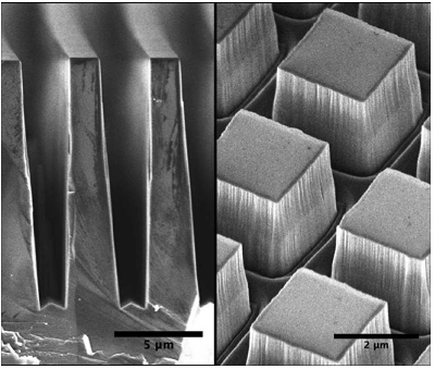
ning electron microscope (SEM). As can be seen in
Fig.
5 the sidewalls have a slight angle of 2.62.8°
from the vertical. Ions deflected in glancing impacts
with the sidewalls cause trenching at the bottom of
the wall. In a narrow groove such as this, trenching
gives rise to the triangular ridge along the center of
the groove.
B. Expected Performances
Cracking the sample is naturally not possible for the
final HWPs. For these an estimate of the depth was
acquired by comparing several SEM images taken at
different angles. The distance between two recogniz-
able features, one at the top and one at the bottom of
a groove, was measured in micrographs recorded at
tilt angles between 5 and 26°. From the variation in
this distance with angle, the depth could be calcu-
lated. The depth measured by this method on
cracked samples was in good agreement with cross
section images (within 2%). Our prototypes have
met the specifications: line width 1.8 μm (sidewall
angle 2.7°), period 4.6 μm, and depth 13.7 μm. As
shown in Fig.
6, the retardance of the manufactured
HWP is nearly ideal in the center of the spectral
band. The mean and standard deviation of the phase
shift over the whole upper N-band (1113.2 μm)
equal 3.143 0.061 rad (180 .08 3.51 °).
C. Antireflective Grating (ARG)
Incoherent reflections with different phase shift may
interfere with the main beam and degrade perfor-
mance of the component. The natural reflection of
the diamond at N-band is 17% for one interface.
Although the achromatic HWP was not designed
with reducing reflections in mind, it still serves this
purpose to some degree. As shown in Fig.
7, the the-
oretical transmittance is quite good between 11.5
and 13 μm because the diffraction grating actually
acts as an antireflective layer at this wavelength.
Fig. 4. (Color online) RCWA multiparametric simulation: mean (left) and standard deviation (right) of the RMS phase shift error
(logarithmic scale) over the upper N-band, with α ranging from 2.6 to 2.8°. The period is set to Λ 4.6 μm (SWG limit).
Fig. 5. SEM-micrographs of a diamond achromatic HWP. Left:
cross sectional view of the grooves. Right: antireflective structure
on the backside.
5900 APPLIED OPTICS / Vol. 51, No. 24 / 20 August 2012

In addition, an ARG was designed to reduce sur-
face reflections using a diffraction grating analysis
program (GSOLVER, version 4.20c., Grating Solver
Development Co., USA). The program uses algo-
rithms based on RCWA to calculate values of the
zero-order transmission. A 2D SWG formed by bin-
ary square (2.6 × 2.6 × 2 μm) shaped structures
with a 4 μm period was etched on the backside of
the HWP to reduce the reflection from 17% to less
than 0.5% in the wavelength region of interest (see
Fig.
8). Etching the ARG was much less demanding
than the HWP structure, bu t there is still trenching
and the sidewalls are not perfectly vertical [
11]
(Fig.
5). Since there was some deviation from the
calculated structure, the etch time was optimized
by testing the performance. The transmittance of
diamond substrates with a single sided ARG was
measured in a Perkin Elmer 983 infrared spectro-
photometer. Afte r removing the effects of interfer-
ence within the sample and comparing with an
unetched sample, the transmittance of a single AR
interface has been determined (Fig.
8). As can be
seen, the bandwidth of the manufactured structure
was slightly larger than the calculated one. This
may be due to the somewhat tilted sidewalls. The
total transmittance of the finished HWP components
was between 89% and 95% over the band.
6. Conclusion and Directions for Future Research
Diamond is a good material for manufacturing achro-
matic HWPs for mid-IR wavelengths. By optimiz-
ing the gratings with manufacturing limitations in
mind, components dedicated to the upper N-band
(12 μm) could be achieved including an antireflec-
tive solution on their backside. Diamond HWPs are
likely to be used for many applications, particularly
for optical vortices in astrophysics. The diamond
HWP shown in this paper has been developed to en-
able the manufacturing of an N-band annular groove
phase mask (AGPM), which will be installed in 2012
on the VISIR instrument at the VLT, and is also an
excellent candidate for METIS at the future Eur-
opean Extremely Large Telescope. This specific ap-
plication will be the subject of a forthcoming paper.
Moreover, a new process using e-beam lithography
is now being explored to reach smaller grating peri-
ods, and thereby shorter operating wavelengths.
These AGPMs are being evaluated for implementa-
tion on high-contrast imaging instruments such as
NACO (L-ban d 3.8 μm) and SPHERE (K-band
2.2 μm) at the Very Large Telescope in Chile.
The first author is grateful to the financial sup-
port of the Belgian Fonds de la Recherche Scientifi-
que (FRIA) and Fonds de solidarité ULg. We also
gratefully acknowledge financial support from the
Swedish Diamond Center (financed by Uppsala
University), and the Communauté française de
Fig. 7. Transmission spectrum of a SWG etched on diamond
with HWP optimal specifications, with sidewall angle (2.62.8°).
The dotted line shows the natural transmission of the diamond
at N-band, without the SWG (83%).
Fig. 8. Transmission spectrum of one diamond interface with
ARG measured with a spectrophotometer. The calculated trans-
mission values for three different depths are also shown.
Fig. 6. (Color online) Retardance for a diamond HWP with opti-
mal specifications at α 2.62.8° (slope of the walls). Bandwidth:
1113.2 μm.
20 August 2012 / Vol. 51, No. 24 / APPLIED OPTICS 5901

Citations
More filters
Patent
21 Jan 2016
TL;DR: In this paper, a system for magnetic detection includes a nitrogen vacancy (NV) diamond material comprising a plurality of NV centers, a radio frequency (RF) excitation source configured to provide RF excitation to the NV diamond material, an optical detector configured to receive an optical signal emitted by the NVD material, and a controller.
Abstract: A system for magnetic detection includes a nitrogen vacancy (NV) diamond material comprising a plurality of NV centers, a radio frequency (RF) excitation source configured to provide RF excitation to the NV diamond material, an optical excitation source configured to provide optical excitation to the NV diamond material, an optical detector configured to receive an optical signal emitted by the NV diamond material, and a controller. The optical signal is based on hyperfine states of the NV diamond material. The controller is configured to detect a gradient of the optical signal based on the hyperfine states emitted by the NV diamond material.

77 citations

Journal ArticleDOI
TL;DR: In this paper, the annular groove phase mask (AGPM) was designed to produce a vortex effect in the L band, and etched it onto a series of diamond substrates.
Abstract: Context. Coronagraphy is a powerful technique to achieve high contrast imaging, hence to image faint companions around bright targets. Various concepts have been used in the visible and near-infrared regimes, while coronagraphic applications in the mid-infrared nowadays remain largely unexplored. Vector vortex phase masks based on concentric subwavelength gratings show great promise for such applications. Aims. We aim at producing and validating the first high-performance broadband focal plane phase mask coronagraphs for applications in the mid-infrared regime, and in particular the L band with a fractional bandwidth of ∼16% (3.5–4.1 μm). Methods. Based on rigorous coupled wave analysis, we designed an annular groove phase mask (AGPM) producing a vortex effect in the L band, and etched it onto a series of diamond substrates. The grating parameters were measured by means of scanning electron microscopy. The resulting components were then tested on a mid-infrared coronagraphic test bench. Results. A broadband raw null depth of 2 × 10 −3 was obtained for our best L-band AGPM after only a few iterations between design and manufacturing. This corresponds to a raw contrast of about 6 × 10 −5 (10.5 mag) at 2λ/D. This result is fully in line with our projections based on rigorous coupled wave analysis modelling, using the measured grating parameters. The sensitivity to tilt and focus has also been evaluated. Conclusions. After years of technological developments, mid-infrared vector vortex coronagraphs have finally become a reality and live up to our expectations. Based on their measured performance, our L-band AGPMs are now ready to open a new parameter space in exoplanet imaging at major ground-based observatories.

77 citations


Cites background or methods from "Design, manufacturing, and performa..."

  • ...We have recently shown (Delacroix et al. 2012b) that diamond is a good material for manufacturing achromatic half-wave plates for mid-infrared wavelengths (e.g., L and N bands centred respectively around 3.8 µm and 10 µm)....

    [...]

  • ...This process was painstakingly optimised to achieve the high pattern homogeneity, precision and aspect ratio necessary for half-wave plates and AGPMs in the N band (Delacroix et al. 2012a)....

    [...]

Patent
21 Jan 2016
TL;DR: In this article, a propulsion unit and a steering unit are coupled with a processor to determine a vector of one or more magnetic fields and a processor is further configured to cause the steering unit to direct the device toward the electrical power transmission line.
Abstract: A device includes a propulsion unit configured to move the device and a steering unit configured to control the direction of the device. The device also includes a power unit configured to provide power to the propulsion unit and a charging unit configured to use an electric field to provide electrical power to the power unit. The device further includes a first magnetic sensor configured to determine a vector of one or more magnetic fields and a processor communicatively coupled to the propulsion unit, the steering unit, the power unit, and the magnetic sensor. The processor is configured to receive, from the magnetic sensor, a time-varying signal indicative of a magnetic field and determine, based on the time-varying signal, that the magnetic field is associated with an electrical power transmission line. The processor is further configured to cause the steering unit to direct the device toward the electrical power transmission line.

71 citations

Journal ArticleDOI
TL;DR: In this paper, a process for fabricating high aspect ratio gratings in single or polycrystalline diamond with the high precision required by micro-optics is described, which is similar to our approach.

60 citations

Patent
21 Jan 2016
TL;DR: In this paper, a system for magnetic detection of an external magnetic field is described, which includes a nitrogen vacancy (NV) diamond material comprising a plurality of NV centers, a magnetic field generator that generates magnetic field, a radio frequency (RF) excitation source that provides RF excitation, an optical detector that receives an optical signal emitted by the NV diamond material, and a controller.
Abstract: A system for magnetic detection of an external magnetic field is disclosed. The system includes a nitrogen vacancy (NV) diamond material comprising a plurality of NV centers, a magnetic field generator that generates a magnetic field, a radio frequency (RF) excitation source that provides RF excitation, an optical excitation source that provides optical excitation, an optical detector that receives an optical signal emitted by the NV diamond material, and a controller. The controller is configured to calculate a control magnetic field, control the magnetic field generator to generate the control magnetic field, receive a light detection signal from the optical detector based on the optical signal due to the sum of the generated control magnetic field and the external magnetic field, store measurement data based on the received light detection signal, and calculate a vector of the external magnetic field based on the stored measurement data.

55 citations

References
More filters
Journal ArticleDOI
TL;DR: In this article, a rigorous coupled-wave approach is used to analyze diffraction by general planar gratings bounded by two different media, and the analysis is based on a state-variables representation and results in a unifying, easily computer-implementable matrix formulation.
Abstract: A rigorous coupled-wave approach is used to analyze diffraction by general planar gratings bounded by two different media. The grating fringes may have any orientation (slanted or unslanted) with respect to the grating surfaces. The analysis is based on a state-variables representation and results in a unifying, easily computer-implementable matrix formulation of the general planar-grating diffraction problem. Accurate diffraction characteristics are presented for the first time to the authors’ knowledge for general slanted gratings. This present rigorous formulation is compared with rigorous modal theory, approximate two-wave modal theory, approximate multiwave coupled-wave theory, and approximate two-wave coupled-wave theory. Typical errors in the diffraction characteristics introduced by these various approximate theories are evaluated for transmission, slanted, and reflection gratings. Inclusion of higher-order waves in a theory is important for obtaining accurate predictions when forward-diffracted orders are dominant (transmission-grating behavior). Conversely, when backward-diffracted orders dominate (reflection-grating behavior), second derivatives of the field amplitudes and boundary diffraction need to be included to produce accurate results.

2,224 citations


"Design, manufacturing, and performa..." refers methods in this paper

  • ...RCWA is an analysis method that is applicable to any multilayer grating profile [12,13]....

    [...]

Journal ArticleDOI
Lifeng Li1
TL;DR: In this paper, a numerically stable method for the analysis of diffraction gratings of arbitrary profile, depth, and in conical mountings is presented based on the classical modal method and uses a stack of lamellar gratittivity to approximate an arbitrary profile.
Abstract: A numerically stable method is presented for the analysis of diffraction gratings of arbitrary profile, depth, and in conical mountings. It is based on the classical modal method and uses a stack of lamellar gratpermittivity to approximate an arbitrary profile. A numerical procedure known as the R-matrix propagation aling layers gorithm is used to propagate the modal fields through the layers. This procedure renders the implementation of this new method completely immune to the numerical instability that is associated with the conventional algorithm. Numerical examples including diffraction efficiencies of both dielectric and metallic propagation gratings of depths that range from subwavelength to hundreds of wavelengths are presented. Information about the convergence and the computation time of the method is also included.

361 citations


"Design, manufacturing, and performa..." refers methods in this paper

  • ...RCWA is an analysis method that is applicable to any multilayer grating profile [12,13]....

    [...]

Journal ArticleDOI
TL;DR: This achromatic wave plate demonstrates a huge frequency bandwidth (upsilonmax/upsilonmin approximately 7), and therefore can be applied to terahertz time domain spectroscopy and polarimetry.
Abstract: Phase retarders usually present a strong frequency dependence. We discuss the design and characterization of a terahertz achromatic quarter-wave plate. This wave plate is made from six birefringent quartz plates precisely designed and stacked together. Phase retardation has been measured over the whole terahertz range by terahertz polarimetry. This achromatic wave plate demonstrates a huge frequency bandwidth (upsilonmax/upsilonmin approximately 7), and therefore can be applied to terahertz time domain spectroscopy and polarimetry.

268 citations


"Design, manufacturing, and performa..." refers methods in this paper

  • ...Another way of achieving broadband performance is stacking several crystal wave plates together [2] and orienting their birefringent axes using a Pancharatnam method [3]....

    [...]

Journal ArticleDOI
01 Apr 1955
TL;DR: In this paper, an achromatic quarter-wave plate is obtained by superposing three birefringent plates of the same material; the first and last should have the same retardation 2δ1 their fast vibration directions being parallel to one another but inclined at a specific angle c to that of the central plate-of retardation π.
Abstract: An achromatic quarter-wave plate is obtained by superposing three birefringent plates of the same material; the first and last should have the same retardation 2δ1 their fast vibration directions being parallel to one another but inclined at a specific angle c to that of the central plate-of retardation π. The desired range of achromatism determines the optimum values of 2δ1 and c (which, in turn, will determine the orientation of the effective principal planes of the combination). As an example, using mica retardation plates prepared for Hg 5461, the range from 4100 A to 6800 A is covered with 2δ1 = 115° 42' and c = 69° 54'. Further, for a particular wave-length, a birefringent compensator of variable retardation (0 to 2π) is obtained by interposing a half-wave plate that can be rotated in its own plane, between two quarter-wave plates that have their fast vibration directions parallel. The results follow from the Poincare sphere by geometrically compounding successive rotations.

230 citations

Journal ArticleDOI
01 Apr 1955
TL;DR: In this article, two half-wave plates and one quarter-wave plate are superposed on the same material, such that the fast vibration-directions of the successive plates make specific angles with the azimuth of the linear vibration incident on the first plate.
Abstract: Circularly polarised light is obtained by superposing two half-wave plates and one quarter-wave plate, all of the same material, such that the fast vibration-directions of the successive plates make specific angles θ1, θ2, θ3 with the azimuth of the linear vibration incident on the first plate The required range of achromatism determines the optimum values of the angles Thus, using mica retardation plates prepared for Na 5890, the range from 4000 A to 7800 A is covered with θ1 = 6° 52′, θ2 = 34° 32′, θ3 = 100° 20′; while the range 4400 A to 7400 A can be covered with superior achromatism by taking θ1 = 6° 30′, θ2 = 34° 34′, θ3 = 101° 8′

200 citations

Frequently Asked Questions (24)
Q1. What are the contributions in "Design, manufacturing, and performance analysis of mid-infrared achromatic half-wave plates with diamond subwavelength gratings" ?

In this paper, the authors present a solution for creating robust monolithic achromatic half-wave plates ( HWPs ) for the infrared, based on the form birefringence of subwavelength gratings ( SWGs ) made out of diamond. 

The diamond HWP shown in this paper has been developed to enable the manufacturing of an N-band annular groove phase mask ( AGPM ), which will be installed in 2012 on the VISIR instrument at the VLT, and is also an excellent candidate for METIS at the future European Extremely Large Telescope. 

The phase retardation ΔΦ introduced by a birefrin-gent SWG between the two polarization components is dependent on the wavelength, and is given byΔΦTE–TM λ 2π λ Δnform λ ; (2)whereΔnform λ nTE λ − nTM λ : (3)h is the optical path through the birefringent medium. 

By optimizing the gratings with manufacturing limitations in mind, components dedicated to the upper N-band (∼12 μm) could be achieved including an antireflective solution on their backside. 

For the longest wavelengths (N-band mostly), the aspect ratio ρ is much lower for high refractive indices (>2.25), while for the shorter wavelengths, the filling factor F varies strongly, which results in a very fluctuating aspect ratio due to its definition as a minimum of either the wall or void thickness. 

By varying the grating parameters (geometry, material, incidence), the wavelength dependence in Δnform should be tuned to be closely proportional to the wavelength across a wide spectral band. 

the demand for instruments in the mid-infrared (L-band ∼3.8 μm, M-band ∼4.8 μm, N-band ∼10.5 μm) is increasing in many domains of astrophysics. 

SWGs are micro-optical structures with a period Λ smaller than λ ∕ n, λ being the observed wavelength of the incident light and n the refractive index of the grating substrate. 

The authors conclude that using substrates with high refractive indices (e.g., diamond,ZnSe, Ge) can make the microfabrication of SWGs for achromatic HWPs much easier. 

Among the materials commonly used in the Nband, one good candidate is diamond, with a refractive index ∼2.38 for the region of interest (from 3 to 13 μm). 

Another way of achieving broadband performance is stacking several crystal wave plates together [2] and orienting their birefringent axes using a Pancharatnam method [3]. 

Many new optical devices have been made with SWGs, such as high-efficiency diffraction gratings, polarization-selective gratings, wave plates, and monolithic antireflective structures [11]. 

a large spectral bandwidth is needed in many cases, especially in astrophysics, both to increase the signal-to-noise ratio and to allow spectrophotometry. 

The diamond HWP shown in this paper has been developed to enable the manufacturing of an N-band annular groove phase mask (AGPM), which will be installed in 2012 on the VISIR instrument at the VLT, and is also an excellent candidate for METIS at the future European Extremely Large Telescope. 

The larger periods and lower aspect ratios of the N-band HWP should make this grating easier to fabricate compared to bands of shorter wavelengths, as shown in Section 3. 

In astrophysics, when it comes to observing a very high-contrast scene, one must be able to cancel the bright source, or at least drastically reduce its intensity. 

This attenuation can be achieved by combining two portions of the incident light beam, one of which having to undergo a half wavelength (or π) phase shift. 

A birefringent medium, such as a grating (see Fig. 1), has two different refractive indices, nTE and nTM, with regard to the polarization states TE (transverse electric, parallel to the grating grooves) and TM (transverse magnetic, orthogonal to the grating grooves). 

In the first20 August 2012 / Vol. 51, No. 24 / APPLIED OPTICS 5899approximation, one can tell that the relation between the optimum line width and depth is quasi linear, with a regression coefficient approximately equal to 10. 

The mean and standard deviation of the phase shift over the whole upper N-band (11–13.2 μm) equal ∼3.143 0.061 rad (180.08 3.51°). 

A 2D SWG formed by binary square (2.6 × 2.6 × 2 μm) shaped structures with a 4 μm period was etched on the backside of the HWP to reduce the reflection from 17% to less than 0.5% in the wavelength region of interest (see Fig. 8). 

The retardance of a zero-order wave plate varies hyperbolically with thewavelength, which limits the operation of single wave plates to monochromatic light. 

After removing the effects of interference within the sample and comparing with an unetched sample, the transmittance of a single AR interface has been determined (Fig. 8). 

The solution corresponds to the reflection and transmission matrices in the two modes (TE/TM), describing the entire diffractive characteristics of the simulated structure: the diffraction efficiencies (η m TE ) and (η m TM), and the phase shift (ΔΦTE–TM).