scispace - formally typeset
Search or ask a question
Journal ArticleDOI

Design, Optimization, and Scaling of MEM Relays for Ultra-Low-Power Digital Logic

TL;DR: In this paper, a sensitivity-based energy-delay optimization approach is developed in order to establish simple relay design guidelines, and it is found that, at the optimal design point, every 2 X energy increase can be traded off for a ~1.5x reduction in relay delay.
Abstract: Microelectromechanical relays have recently been proposed for ultra-low-power digital logic because their nearly ideal switching behavior can potentially enable reductions in supply voltage (Vdd) and, hence, energy per operation beyond the limits of MOSFETs. Using a calibrated analytical model, a sensitivity-based energy-delay optimization approach is developed in order to establish simple relay design guidelines. It is found that, at the optimal design point, every 2 X energy increase can be traded off for a ~1.5x reduction in relay delay. A contact-gap-to-actuation-gap thickness ratio of 0.7-0.8 is shown to result in the most energy-efficient relay operation, implying that pull-in operation is preferred for an energy-efficient relay design. Based on the analytical model and design guidelines, a scaling theory for relays is presented. A scaled relay technology is projected to provide >; 10 X energy savings over an equivalent MOSFET technology, for circuits operating at clock frequencies up to ~100 MHz.

Summary (3 min read)

Introduction

  • This has forced the supply voltage (Vdd) to remain relatively constant across CMOS technology generations, causing power density to increase with transistor density and thus limiting the performance benefits of transistor scaling [1].
  • In order to arrive at the proposed methodology, Section II begins this paper by developing a general model for relay logic delay and energy that is calibrated to experimental data.

II. LOGIC RELAY ENERGY–DELAY MODEL

  • The principle and analytical models for MEM relay operation are described to provide the necessary 0018-9383/$26.00 © 2010 IEEE background for a subsequent discussion of design optimization and scaling.
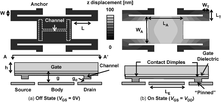
  • A metallic channel electrode is attached underneath the gate electrode via an intermediary gate dielectric layer.
  • In the case of a 4T relay, although the device turns on when |Vgb| increases above Vpi, it turns off when |Vgb| is lowered below the “release voltage” (Vrl).
  • The hysteretic switching behavior (Vrl < Vpi) occurs for “pull-in-mode” operation (wherein Felec remains larger than Fspring for values of Vrl < |Vgb| < Vpi when the channel is in contact with the source/drain electrodes) and is exacerbated by surface adhesion force (FA) in the contact regions.
  • The as- fabricated air gap in the contacting region (gd) can be made to be smaller than the as-fabricated air gap in the actuation region (g) to reduce the hysteresis voltage.

A. Switching Voltages

  • The relay switching voltages can be derived by balancing the electrostatic force against the spring restoring force.
  • The first prototype 4T relay design reported in [10] suffers from gate dielectric charging issues, leading to unwanted parasitic actuation effects as well as undesirable influence on gate switching voltages and pull-in time.
  • This is because the mechanical design and models of energy and performance for 4T and 3T relays are essentially identical.
  • This is within 2× of the ∼0.2-μN FA value obtained via atomic force microscopy measurements [19].

B. Turn-On Delay

  • For RF relays which employ micrometer-scale actuation gaps, Q is limited by squeeze-film damping.
  • It has been shown that Q decreases linearly with beam thickness and is independent of the beam width and beam length [21], [22].
  • In fact, it may be preferable to avoid high-Q relay designs to minimize non-ideal switching effects such as contact bounce and long settling time.

C. Switching Energy

  • The energy consumed in switching a relay is supplied by the voltage source which charges/discharges capacitances.
  • By using the calibrated delay and energy models, the switching voltages, delay, and energy for relays with various design parameters can be predicted.
  • These, in turn, can be used for relay circuit design optimization.

III. RELAY ENERGY–DELAY OPTIMIZATION

  • Since the switching delay of a relay is dominated by its mechanical delay rather than its electrical delay, an optimized relay-based circuit design should utilize complex gates [8] such that all the relays move simultaneously and only one mechanical delay is incurred per operation.
  • In optimizing a relay circuit design, it is important to note that, as for a CMOS circuit design [23]–[28], energy and delay are traded off by adjusting various device design parameters.
  • The energy-delay tradeoff is optimized essentially by solving the following constrained optimization problem for the N-relay complex gate: Minimize : tdelay ∼= α √ meff keff ( gd g )γ ( Vdd Vpi − χ )−β.
  • In a complex gate, not all the nodes (i.e., capacitances) switch with equal probability; therefore the authors can generalize the circuit to have an average activity.

A. Sensitivity Analysis

  • CMOS integrated circuit optimization utilizing energy-delay sensitivity analysis has been described extensively in [23]–[28], so only the key concepts are briefly reviewed here.
  • 1) Sensitivity to Supply Voltage (Vdd): As Vdd increases, the switching delay decreases because the electrostatic force increases, but the switching energy increases.
  • Where tdelay and Es are the delay and energy, respectively, at a given Vdd and Vnorm = βVdd/(Vdd − χVpi).

B. Relay Design Optimization

  • An optimized relay design is reached by balancing the various sensitivities to the design variables.
  • As a result, the optimal fixed-to-area-dependent capacitance ratio is less than one, as shown in Fig. 14.6 5) Relay Design Optimization Procedure:.
  • From the results of the sensitivity analysis, the following simple relay design optimization procedure (illustrated in Fig. 16) can be established.
  • 4) Finally, the optimal beam length is calculated to result in the optimal Vpi.
  • To provide a concrete example, this procedure is applied to optimize the design of a 5-μm-wide relay (with the parameters shown in Table I) for a nominal switching energy Es = 2 pJ and an average fixed capacitance CL ranging from 10 to 100 fF.

C. Energy-Efficiency Limit

  • For ultra-low-power electronics applications such as wireless sensor networks, switching energy [32] rather than speed is the primary concern.
  • The minimum switching energy for relays is dictated by the need for the spring restoring force to overcome the surface adhesion energy (Γ) in the ON state, in order to break physical contact 0.5keffg 2 d ≥ Γ. (24).
  • In other words, the minimum spring stiffness is keff = 2Γ/g2d.
  • Of course, the switching energy will be higher for any realistic relay design since operation with Vrl = 0 V and Vdd = Vpi provides for no noise margin and thus would be highly impractical.

IV. SCALING IMPLICATIONS

  • Relay miniaturization is desirable for improved device density and reduced operating voltage.
  • Surface adhesion energy and, therefore, the minimum relay switching energy improve by S2.
  • Since the total capacitance is reduced by S and the switching energy improves by S2, the supply voltage can be scaled down by S0.5.
  • Given that relay circuits would be used for applications with clock frequencies up to ∼100 MHz, it is of practical interest to compare them against subthreshold-CMOS circuits (operated with Vdd < VT ), which are designed to operate with very low power consumption [6], [32].

V. CONCLUSION

  • Circuit-level energy-performance analysis is necessary to evaluate the promise of any new device technology for potentially overcoming the energy-efficiency limitations of CMOS technology.
  • For a given contact dimple gap thickness, the optimal dimple-gap thickness to actuation-gap thickness ratio is roughly 0.7, meaning that pull-in operation is preferred for energy-efficient relay design.
  • Specifically, a lower bound for Vcpi can be derived by modeling the movable plate as a beam pinned at the two contact dimple regions.
  • G. M. Rebeiz, RF MEMS, Theory, Design and Technology.

Did you find this useful? Give us your feedback

Figures (23)

Content maybe subject to copyright    Report

236 IEEE TRANSACTIONS ON ELECTRON DEVICES, VOL. 58, NO. 1, JANUARY 2011
Design, Optimization, and Scaling of MEM Relays
for Ultra-Low-Power Digital Logic
Hei Kam, Member, IEEE, Tsu-Jae King Liu, Fellow, IEEE, Vladimir Stojanovi
´
c, Member, IEEE ,
Dejan Markovi
´
c, Member, IEEE, and Elad Alon, Member, IEEE
Abstract—Microelectromechanical relays have recently been
proposed for ultra-low-power digital logic because their nearly
ideal switching behavior can potentially enable reductions in
supply voltage (V
dd
) and, hence, energy per operation beyond
the limits of MOSFETs. Using a calibrated analytical model, a
sensitivity-based energy–delay optimization approach is developed
in order to establish simple relay design guidelines. It is found
that, at the optimal design point, every 2× energy increase can be
traded off for a 1.5× reduction in relay delay. A contact-gap-to-
actuation-gap thickness ratio of 0.7–0.8 is shown to result in the
most energy-efficient relay operation, implying that pull-in opera-
tion is preferred for an energy-efficient relay design. Based on the
analytical model and design guidelines, a scaling theory for relays
is presented. A scaled relay technology is projected to provide
> 10× energy savings over an equivalent MOSFET technology,
for circuits operating at clock frequencies up to 100 MHz.
Index Terms—Digital integrated circuits, logic devices, low
power circuit, microelectromechanical systems, microswitches,
subthreshold slope, 60 mV/dec.
I. INTRODUCTION
O
VER the past 40 years, MOSFET feature size scaling has
resulted in dramatic improvements in the performance,
cost per function, and energy efficiency of integrated circuits.
Due to the fact that the
OFF-state leakage current (I
OFF
) of a
MOSFET increases exponentially with threshold voltage (V
T
),
V
T
can no longer be reduced along with transistor physical
dimensions. This has forced the supply voltage (V
dd
) to remain
relatively constant across CMOS technology generations, caus-
ing power density to increase with transistor density and thus
limiting the performance benefits of transistor scaling [1].
The fundamental cause of the CMOS power density issue
is that the subthreshold swing of a MOSFET (i.e., the rate
at which the transistor turns on/off with increasing/decreasing
Manuscript received June 29, 2010; revised September 8, 2010; accepted
September 23, 2010. Date of publication November 11, 2010; date of current
version December 27, 2010. This work was supported in part by the C2S2 and
MSD Focus Centers (two of the five research centers funded under the Focus
Center Research Program, which is a Semiconductor Research Corporation
program) and in part by a DARPA/MTO NEMS program. The work of E. Alon
was supported by the Berkeley Wireless Research Center under the National
Science Foundation Infrastructure Grant 0403427. The review of this paper was
arranged by Editor A. M. Ionescu.
H. Kam was with the University of California at Berkeley, Berkeley, CA
94720-1770 USA. He is now with Intel Corporation, Hillsboro, OR 97124 USA
(e-mail: heikam@eecs.berkeley.edu).
T.-J. K. Liu, and E. Alon are with the University of California
Berkeley, Berkeley, CA 94720-1770 USA (e-mail: tking@eecs.berkeley.edu;
elad@eecs.berkeley.edu).
V. Stojanovi
´
c is with the Massachusetts Institute of Technology, Cambridge,
MA 02139-4307 USA (e-mail: vlada@mit.edu).
D. Markovi
´
c is with the University of California at Los Angeles, Los
Angeles, CA 90095 USA (e-mail: dejan@ee.ucla.edu).
Digital Object Identifier 10.1109/TED.2010.2082545
gate voltage) is directly proportional to the thermal voltage
(k
B
T/q) which does not scale with transistor dimensions.
Therefore, alternative transistor designs that can achieve steeper
switching behavior than a MOSFET have been proposed to
alleviate this issue [2]–[5]. However, any CMOS or CMOS-
like technology will have a lower limit in energy per operation
due to I
OFF
[6]. To overcome this limit, microelectromechan-
ical (MEM) switches have been investigated for digital logic
applications [7]–[11] because they ideally offer zero I
OFF
and perfectly abrupt switching behavior. In principle, then, the
threshold voltage of a MEM switch (and therefore V
dd
) can be
reduced to be close to 0 V to provide for very low active power
consumption.
In terms of device structure and operation, a MEM relay
designed for digital logic applications [10] is very similar to
relays designed for radio-frequency (RF) signal switching ap-
plications [12]–[15]. However, the contact resistance (R
on
) for
a logic relay can be as high as 10 kΩ (for a load capacitance of
10–100 fF) because the switching delay of a relay-based circuit
is dominated by the mechanical pull-in time (t
pi
, typically
10–100 ns) rather than the electrical charging/discharging delay
(t
RC
) [8], [11]. Thus, R
on
can be traded off for improved
endurance, for example, by utilizing TiO
2
-coated tungsten con-
tacting electrodes to attain high device yield and endurance
> 1 billion switching cycles [10], [11]. This insight enabled the
successful demonstration of the first relay-based logic, memory,
and clocking integrated circuits [16].
Whereas previous papers mainly focused on relay fabri-
cation process optimization [10], [11] and prototype circuit
demonstrations [8], [16], this paper focuses on developing
a methodology for an energy–performance optimized relay
design. Similarly to MOSFETs, dimensional scaling can be
applied to relays to improve device density (for lower cost
per function), switching delay (for higher performance), and
power consumption (for improved energy efficiency). This
paper therefore also examines the implications of scaling relay
devices while following the proposed design methodology.
In order to arrive at the proposed methodology, Section II
begins this paper by developing a general model for relay
logic delay and energy that is calibrated to experimental data.
Section III then utilizes this model to establish a sensitivity-
based energy-delay optimization methodology as well as a
simplified relay device design procedure. Based upon these
design guidelines, a scaling theory for relays is presented in
Section IV. Conclusions are provided in Section V.
II. L
OGIC RELAY ENERGY–DELAY MODEL
In this section, the principle and analytical models for
MEM relay operation are described to provide the necessary
0018-9383/$26.00 © 2010 IEEE

KAM et al.: DESIGN, OPTIMIZATION, AND SCALING OF MEM RELAYS FOR DIGITAL LOGIC 237
Fig. 1. Schematic 3-D view of the electrostatically actuated 4T relay structure.
background for a subsequent discussion of design optimization
and scaling. Fig. 1 shows a schematic 3-D view of an elec-
trostatically actuated four-terminal (4T) relay [10], with key
design parameters shown in Fig. 2 and Table I. The voltage
applied between the movable gate electrode and the fixed body
electrode determines whether current can flow between the
source and drain electrodes. The gate electrode is supported
by four suspended beams (with an effective spring constant
k
eff
) anchored to the substrate at four corners. A folded-flexure
beam design is used to reduce the effects of residual/thermal
stress and vertical strain gradient. A metallic channel electrode
is attached underneath the gate electrode via an intermediary
gate dielectric layer.
The position of the gate stack depends on the electric field
across the actuation gap between the gate and the body elec-
trode, i.e., the balance between the electrostatic attractive force
(F
elec
) and the spring restoring forces of the beams (F
spring
).
In the
OFF state [Fig. 2(a)], an air gap separates the channel
from the coplanar source/drain electrodes so that no current can
flow. In the
ON state [Fig. 2(b)], the gate stack is “pulled in”
by the electrostatic force between the gate and the body so that
the channel contacts the source/drain electrodes in the contact
dimple regions, allowing current to flow.
The electrical transition between
OFF and ON states is abrupt,
i.e., current flow between the source and drain electrodes in-
creases abruptly as the gate-to-body voltage (V
gb
) increases
above the “pull-in voltage” (V
pi
). Since the electrostatic at-
tractive force is ambipolar, a 4T relay can be turned on either
by applying a positive gate-to-body voltage (mimicking the
operation of an n-channel MOSFET, e.g., with the body biased
at the ground) or by applying a negative gate-to-body voltage
(mimicking the operation of a p-channel MOSFET, e.g., with
the body biased at V
dd
).
The absolute value of the voltage at which a mechanical
switch turns off is usually smaller than that of the voltage at
which it turns on, i.e., the IV characteristics of a mechanical
switch exhibit some hysteresis. In the case of a 4T relay,
although the device turns on when |V
gb
| increases above V
pi
,
it turns off when |V
gb
| is lowered below the “release voltage”
(V
rl
). The hysteretic switching behavior (V
rl
<V
pi
) occurs for
“pull-in-mode” operation (wherein F
elec
remains larger than
F
spring
for values of V
rl
< |V
gb
| <V
pi
when the channel is
in contact with the source/drain electrodes) and is exacerbated
by surface adhesion force (F
A
) in the contact regions. The as-
fabricated air gap in the contacting region (g
d
) can be made to
be smaller than the as-fabricated air gap in the actuation region
(g) to reduce the hysteresis voltage. This dimpled contact
design is also beneficial to precisely define the area of the con-
tacting region and to reduce the device turn-on delay (t
delay
).
To provide insight into relay operation and guidance for relay
scaling, analytical models for relay performance parameters are
needed. The most relevant physical properties and equations
governing relay behavior such as pull-in voltage, release volt-
age, and turn-on delay are briefly reviewed here, and measured
data
1
for devices with design parameters as shown in Table I
are used for model calibration.
A. Switching Voltages
The relay switching voltages can be derived by balancing the
electrostatic force against the spring restoring force. As will be
derived in the following section, the energy efficiency of a relay
is optimized by operating it in pull-in mode, i.e., designing it
such that g
d
>g/3. In this case, hysteretic switching behavior
will occur, and the hysteresis is exacerbated by surface adhesion
forces. For pull-in-mode operation, the switching voltages are
given by [13], [15]
V
pi
=
8k
eff
g
3
27ε
o
A
V
rl
=
2(k
eff
g
d
F
A
)(g g
d
)
2
ε
o
A
(1)
where k
eff
is the effective spring constant of the movable
structure and A is the actuation area ( L
A
× W
A
, ignoring
release etch holes). Note that, in (1), non-ideal effects such as
fringing electric fields are assumed to be negligible.
In general, k
eff
decreases with increasing flexure beam length
(L). Thus, V
pi
and V
rl
can be adjusted via a lithographic mask
design, and different values of V
pi
and V
rl
can be achieved
for different relays on a single chip. This tunability allows the
circuit designer to make direct tradeoffs between layout area,
circuit operating speed, and energy efficiency. As was discussed
in [11], the beams exhibit both bending and rotational motions
when the movable plate is actuated downward. A precise k
eff
model that accounts for shear displacement and rotational iner-
tia is complex [17]; by sacrificing some degree of accuracy, k
eff
can be rendered into a more intuitive form consisting of flexural
( 1/L
3
) and torsional ( 1/L) [18] terms
1
k
eff
=
γ
f
EWh
3
L
3
1
+
γ
t
GW h
3
L
1
(2)
where γ
f
and γ
t
are the flexural and torsional constants,
respectively, both of which are roughly fixed for a given relay
technology. Using ANSYS, γ
f
and γ
t
are found to be 3.66 and
1
4T relays have been demonstrated using conventional surface micromachin-
ing processes [10]. However, the first prototype 4T relay design reported in
[10] suffers from gate dielectric charging issues, leading to unwanted parasitic
actuation effects as well as undesirable influence on gate switching voltages
and pull-in time. While research toward resolving this issue is on-going, for
the purpose of developing an accurate analytical model, it is sufficient to use
data for a simpler 3T relay variant (wherein there is no gate dielectric layer,
the movable plate together with the attached metallic electrode serves as the
source electrode, the underlying electrode serves as the gate electrode, and the
coplanar electrodes serve as drain electrodes [11]) to calibrate the analytical
models for pull-in voltage, release voltage, and turn-on delay (t
delay
).Thisis
because the mechanical design and models of energy and performance for 4T
and 3T relays are essentially identical.

238 IEEE TRANSACTIONS ON ELECTRON DEVICES, VOL. 58, NO. 1, JANUARY 2011
Fig. 2. ANSYS-simulated displacement contours and schematic cross-sectional views of the 4T relay structure in the (a) OFF state (V
GS
= 0V) and (b) ON state
(V
GS
= V
DD
).
TAB LE I
D
ESIGN PARAMETERS FOR THE FABRICATED RELAYS
Fig. 3. Measured relay V
pi
versus L. The analytical model matches the
measured data to within 10%.
1.341 × 10
10
m
2
, respectively. With these values and (2), (1)
yields V
pi
values within 10% of the measured data (Fig. 3).
It is important to note that there is an upper bound for the
beam length to ensure that the relay can be turned off. This
length corresponds to the requirement that F
spring
is larger than
F
A
in the ON state. F
A
can be extracted from the measurements
of V
pi
and V
rl
for devices of various beam lengths, according to
the following equation [derived from (1)]:
V
2
rl
=
27
4
g
d
g
1
g
d
g
2
V
2
pi
2(g g
d
)
2
ε
o
A
F
A
. (3)
F
A
is extracted to be 0.45 μN on average for TiO
2
-coated tung-
sten electrodes with a contact dimple area (A
d
) of 2 × 10 μm
2
,
as shown in Fig. 4. This is within 2× of the 0.2-μN F
A
value
obtained via atomic force microscopy measurements [19].
It is also important to note that there is an upper bound
for V
dd
, not only to avoid gate dielectric breakdown in 4T
relays, but also to avoid the undesirable pull-in of the movable
plate to the underlying fixed electrode. For the relay structure
considered in this work, the lower and upper bounds of this
catastrophic pull-in voltage (V
cpi
) can be derived (as shown in
Appendix I) by modeling the movable plate as a beam anchored
at the two contact dimple regions
V
cpi
=
ζ
Eh
3
(g g
d
)
3
ε
o
L
4
A
(4)
where ζ lies within the range from 1.516 to 3.444. For the
switches used in this work, (4) predicts a V
cpi
value in the range

KAM et al.: DESIGN, OPTIMIZATION, AND SCALING OF MEM RELAYS FOR DIGITAL LOGIC 239
Fig. 4. Measured V
2
rl
versus V
2
pi
. F
A
is extracted to be 0.45 μN.
from 14.6 to 33.2 V, which properly bounds the experimentally
measured value of 23 V.
B. Turn-On Delay
When an actuation voltage (V ) is applied between a movable
electrode and a fixed electrode, the motion of the movable
electrode is governed by Newton’s second law of motion,
yielding the following second-order differential equation [20]:
m
eff
¨z +
k
eff
m
eff
Q
˙z + k
eff
z =
ε
o
AV
2
2(g z)
2
. (5)
The right-hand side of the equation represents the electro-
static force, Q is the quality factor, and z is the displacement.
Note that non-ideal effects such as contact bounce and settling
time are assumed to be negligible. To provide insight for relay
design, t
delay
can be approximated in closed form by (derived
in Appendix II)
t
delay
=
α
m
eff
k
eff
g
d
g
γ
V
dd
V
pi
χ
β
,
for 5V
pi
V
dd
> 1.1V
pi
; g
d
g/3(6)
where χ
=
0.8 and m
eff
is the effective mass of transport. This
effective mass consists of the mass of the movable electrode
and the loaded mass of the springs; it can be determined from
the total kinetic energy in the relay (KE
tot
) and the velocity of
the actuation plate (v
p
) [11]
m
eff
=
KE
tot
0.5v
2
p
=
m
p
v
2
p
+
v
2
b
dm
b
v
2
p
=α
o
ρAh+α
1
ρW Lh (7)
where α
o
= 1.8 and α
1
= 2.74, and m
b
and v
b
are the mass and
velocity of the folded beams, respectively.
Equation (6) shows good agreement with the measured pull-
in time, as shown in Fig. 5. As expected intuitively, t
delay
decreases with increasing resonant frequency (
k
eff
/m
eff
)
and “gate overdrive” (V
dd
/V
pi
). t
delay
is also dependent on the
parameters α, β, and γ, which, to first order, depend only on Q.
These parameters (α, β, and γ) are obtained numerically and
are shown in Fig. 6.
It is important to note that β represents the sensitivity of
the delay to V
dd
, and as indicated in Fig. 6, β decreases
with increasing Q. This is because the relay switching speed
Fig. 5. Measured t
delay
versus V
dd
for three different relays.
becomes mass-transport-limited as Q increases. For RF relays
which employ micrometer-scale actuation gaps, Q is limited by
squeeze-film damping. In contrast, for scaled logic relays with
actuation gaps approaching 10 nm, i.e., less than the mean free
path of an air molecule, squeeze-film damping will be negligi-
ble. Rather, the quality factor of nanometer-scale logic relays
will be dominated by surface-related energy-loss mechanisms,
due to their relatively large surface-to-volume ratio. It has been
shown that Q decreases linearly with beam thickness and is
independent of the beam width and beam length [21], [22].
Therefore, it is reasonable to treat Q as a technology-dependent
constant.
It is also important to note that since α, β, and γ saturate
quickly for Q values greater than 1, Q values significantly
higher than 1 do not significantly improve relay performance. In
fact, it may be preferable to avoid high-Q relay designs to min-
imize non-ideal switching effects such as contact bounce and
long settling time. Thus, additional processing/manufacturing
steps to support vacuum packaging may not be necessary.
Subsequently, in this paper, relays with Q 1 will be referred
to as “high-Q relays,” while relays with Q<1 will be referred
to as “low-Q relays.”
C. Switching Energy
The energy consumed in switching a relay is supplied
by the voltage source which charges/discharges capacitances.
These include the capacitance associated with the actuation air
gap, ε
o
A/(g g
d
), and the fixed parasitic capacitance C.In
addition, there will be an actuation-area-dependent extrinsic
capacitance (e.g., due to wire routing). Assuming an area
proportionality factor r and an average relay activity factor a,
the switching energy of a relay can be modeled by the following
equation
2
:
E
switch
=
a ×
εA
g g
d
(1 + r)+C
V
2
dd
. (8)
2
Note that the capacitance associated with the wires used to interconnect a
relay-based circuit would likely scale with
A rather than A. Furthermore,
parasitic interconnect capacitance would likely increase with beam length L.
However, using the linear dependence on A greatly simplifies the calculations,
and the overall findings are relatively unaffected by these simplifications.

240 IEEE TRANSACTIONS ON ELECTRON DEVICES, VOL. 58, NO. 1, JANUARY 2011
Fig. 6. (a) Dependence of α on the quality factor. (b) Dependence of β on the
quality factor. (c) Dependence of γ on the quality factor.
By using the calibrated delay and energy models, the switch-
ing voltages, delay, and energy for relays with various design
parameters can be predicted. These, in turn, can be used for
relay circuit design optimization. For most relay designs, the
beam width W will be the minimum feature size set by pho-
tolithography limitations. The switching delay and energy are
always minimized by utilizing the smallest achievable beam
thickness h and contact dimple gap thickness g
d
, and hence
these two design parameters will be set by process technology
constraints. Once the beam thickness is set, the quality factor
Q [21], [22] and therefore the α, β, and γ values are known.
Fig. 7. (a) Optimized circuit topology for a relay-based logic gate [8]. For
simplicity, only the pull-up network is drawn here. Load capacitance C
i
consists of fixed capacitance C
fix,i
and an area-dependent load capacitance.
(b) Energy-delay optimization problem for a relay-based circuit can be simpli-
fied into optimizing a single relay driving an average fixed capacitance.
Therefore, the supply voltage, actuation area, as-fabricated gap
thickness, and the beam length are the remaining variables for
design optimization.
III. R
ELAY ENERGY–DELAY OPTIMIZATION
Since the switching delay of a relay is dominated by its
mechanical delay rather than its electrical delay, an optimized
relay-based circuit design should utilize complex gates [8]
such that all the relays move simultaneously and only one
mechanical delay is incurred per operation. Thus, relay circuits
with stacked devices are modeled herein, as shown in Fig. 7.
In optimizing a relay circuit design, it is important to note
that, as for a CMOS circuit design [23]–[28], energy and delay
are traded off by adjusting various device design parameters.
The energy-delay tradeoff is optimized essentially by solving
the following constrained optimization problem for the N-relay
complex gate:
Minimize : t
delay
=
α
m
eff
k
eff
g
d
g
γ
V
dd
V
pi
χ
β
Subject to : E
tot
=
N
i=1
a
i
εA
i
g g
d
(1 + r)+C
i
V
2
dd
(9)
where E
tot
is the total energy and A
i
, a
i
, and C
i
are the area,
average activity factor, and the load capacitance of the ith relay
in the complex gate, respectively. In general, all relays have the
same g, g
d
, and r. Furthermore, if we generalize the relay circuit
with an average
3
activity factor a, the total energy consumed by
the circuit can be expressed as
E
tot
= aV
2
dd
εA
tot
g g
d
(1 + r)+C
fix,tot
(10)
where A
tot
and C
fix,tot
are total actuation area and the total
fixed capacitance, respectively. Dividing both sides of (10)
by a · N · (1 + r), one finds that the energy consumption of
relay circuit can be represented by a generalized relay with
3
In a complex gate, not all the nodes (i.e., capacitances) switch with equal
probability; therefore we can generalize the circuit to have an average activity.

Citations
More filters
Journal ArticleDOI
TL;DR: In this paper, a review of the integration of ferroelectrics with 2D materials to implement 2D electron devices is presented, including low-resistance contacts and reliable gate dielectrics.
Abstract: Two-dimensional (2D) materials have the potential to extend state-of-the-art semiconductor technology to sub-nanometer scales and have inspired numerous research efforts exploring novel device structures. The key elements of electron devices, including low-resistance contacts and reliable gate dielectrics, have to be optimized to complete a functional device. This review highlights recent studies on the integration of ferroelectrics with 2D materials to implement 2D electron devices. The high polarization field and ultra-high dielectric constants of ferroelectric materials enable versatile carrier tuning in 2D materials. Various novel device structures and functionalities are enabled with the integration of ferroelectrics and 2D materials. Representative examples, including ferroelectric-gated 2D memory devices, low-power field-effect transistors enabled by high-k ferroelectrics and negative capacitance effect, and optothermal and photoelectronic devices, are reviewed. Current developments and remaining challenges in ferroelectric-gated 2D electron devices are discussed.

63 citations

Journal ArticleDOI
TL;DR: In this paper, the scaling limits of electrostatically actuated nanorelays are explored, and it is shown that adhesion in a nanorelay's contact interface limits its performance with respect to operating voltage, contact resistance, and switching energy.
Abstract: A model to explore the scaling limits of electrostatically actuated nanorelays is presented, which shows that adhesion in a nanorelay's contact interface limits its performance with respect to operating voltage, contact resistance, and switching energy. For logic applications, we show that an ultimately scaled relay can be more efficient than conventional metal-oxide-semiconductor devices if (1) it is designed with very high contact resistances, leading to ≈ 1-MHz operation due to large RC delays, or (2) its actuation area is extremely large compared with its contacting area, leading to very low voltage operation, which reduces overall CV2 losses. We propose new relay scaling relations that account for the scaling of contact interfaces.

57 citations


Cites background or methods from "Design, Optimization, and Scaling o..."

  • ...66g [6], which sets the optimum g for a given gd ....

    [...]

  • ...This energy is derived in [6] as follows:...

    [...]

  • ...Using optimized pass-gate circuit architectures, however, can mitigate the high Us for a scaled nanorelay [5], [6]....

    [...]

  • ...The relay minimizes Us when operated in its pull-in mode [6]; VPI can be estimated as follows:...

    [...]

  • ...Researchers have successfully fabricated operational electrostatic relays at the microscale [2]–[4], as well as relaybased circuits [5], [6]....

    [...]

Proceedings ArticleDOI
01 Dec 2014
TL;DR: In this article, three-dimensional (3D) nano-electro-mechanical (NEM) switches (relays) are proposed to reduce the die area and power consumption of digital logic and memory circuits.
Abstract: Three-dimensional (3-D) nano-electro-mechanical (NEM) switches (relays) are proposed to reduce the die area and power consumption of digital logic and memory circuits.

46 citations

Journal ArticleDOI
TL;DR: This work details the first demonstration of inkjet-printed microelectromechanical (MEM) switches with abrupt switching characteristics, very low on-state resistance, and very low off-state leakage.
Abstract: Printed electronics employing solution-processed materials is considered to be the key to realizing low-cost large-area electronic systems, but the performance of printed transistors is generally inadequate for most of the intended applications due to limited performance of printable semiconductor materials. We propose an alternative approach for a printed switch, where the use of semiconductors can be avoided by building mechanical switches with printed metal nanoparticle-based inks. In this work, we detail the first demonstration of inkjet-printed microelectromechanical (MEM) switches with abrupt switching characteristics, very low on-state resistance (∼10 Ω), and very low off-state leakage. The devices are fabricated using a novel process scheme to build three-dimensional cantilever structures from solution-processed metallic nanoparticles and sacrificial polymer layers. These printed MEM switches thus represent a uniquely attractive path for realizing printed electronics.

46 citations

References
More filters
Book
01 Jan 1928
TL;DR: In this article, the Probleme dynamique and Vibration were used for propagation of ondes reference records created on 2004-09-07, modified on 2016-08-08.
Abstract: Keywords: Probleme dynamique ; Vibration ; Propagation des ondes Reference Record created on 2004-09-07, modified on 2016-08-08

3,839 citations

Journal ArticleDOI
TL;DR: This paper considers the design, fabrication, and characterization of very small Mosfet switching devices suitable for digital integrated circuits, using dimensions of the order of 1 /spl mu/.
Abstract: This paper considers the design, fabrication, and characterization of very small Mosfet switching devices suitable for digital integrated circuits, using dimensions of the order of 1 /spl mu/. Scaling relationships are presented which show how a conventional MOSFET can be reduced in size. An improved small device structure is presented that uses ion implantation, to provide shallow source and drain regions and a nonuniform substrate doping profile. One-dimensional models are used to predict the substrate doping profile and the corresponding threshold voltage versus source voltage characteristic. A two-dimensional current transport model is used to predict the relative degree of short-channel effects for different device parameter combinations. Polysilicon-gate MOSFET's with channel lengths as short as 0.5 /spl mu/ were fabricated, and the device characteristics measured and compared with predicted values. The performance improvement expected from using these very small devices in highly miniaturized integrated circuits is projected.

3,008 citations

Journal ArticleDOI
TL;DR: By replacing the standard insulator with a ferroelectric insulator of the right thickness it should be possible to implement a step-up voltage transformer that will amplify the gate voltage thus leading to values of S lower than 60 mV/decade and enabling low voltage/low power operation.
Abstract: It is well-known that conventional field effect transistors (FETs) require a change in the channel potential of at least 60 mV at 300 K to effect a change in the current by a factor of 10, and this minimum subthreshold slope S puts a fundamental lower limit on the operating voltage and hence the power dissipation in standard FET-based switches. Here, we suggest that by replacing the standard insulator with a ferroelectric insulator of the right thickness it should be possible to implement a step-up voltage transformer that will amplify the gate voltage thus leading to values of S lower than 60 mV/decade and enabling low voltage/low power operation. The voltage transformer action can be understood intuitively as the result of an effective negative capacitance provided by the ferroelectric capacitor that arises from an internal positive feedback that in principle could be obtained from other microscopic mechanisms as well. Unlike other proposals to reduce S, this involves no change in the basic physics of the FET and thus does not affect its current drive or impose other restrictions.

1,722 citations

Journal ArticleDOI
TL;DR: This tutorial paper collects together in one place the basic background material needed to do GP modeling, and shows how to recognize functions and problems compatible with GP, and how to approximate functions or data in a formcompatible with GP.
Abstract: A geometric program (GP) is a type of mathematical optimization problem characterized by objective and constraint functions that have a special form. Recently developed solution methods can solve even large-scale GPs extremely efficiently and reliably; at the same time a number of practical problems, particularly in circuit design, have been found to be equivalent to (or well approximated by) GPs. Putting these two together, we get effective solutions for the practical problems. The basic approach in GP modeling is to attempt to express a practical problem, such as an engineering analysis or design problem, in GP format. In the best case, this formulation is exact; when this is not possible, we settle for an approximate formulation. This tutorial paper collects together in one place the basic background material needed to do GP modeling. We start with the basic definitions and facts, and some methods used to transform problems into GP format. We show how to recognize functions and problems compatible with GP, and how to approximate functions or data in a form compatible with GP (when this is possible). We give some simple and representative examples, and also describe some common extensions of GP, along with methods for solving (or approximately solving) them.

1,215 citations

Book
01 Jan 1967

1,182 citations

Frequently Asked Questions (19)
Q1. What are the contributions mentioned in the paper "Design, optimization, and scaling of mem relays for ultra-low-power digital logic" ?

Based on the analytical model and design guidelines, a scaling theory for relays is presented. 

M. A. Horowitz, E. Alon, D. Patil, S. Naffziger, R. Kumar, and K. Bernstein, “ Scaling, power, and the future of CMOS, ” in IEDM Tech. In 1992, she joined the Xerox Palo Alto Research Center, Palo Alto, CA, as a Member of the research staff, where she worked on the research and development of polycrystalline-silicon thin-film transistor technologies for high-performance flat-panel displays. 

Much like transistor scaling, relay miniaturization leads to dramatic improvements in density (for lower cost perfunction), switching delay (for higher performance), and energy efficiency. 

For a given contact dimple gap thickness, the optimal dimple-gap thickness to actuation-gap thickness ratio is roughly 0.7, meaning that pull-in operation is preferred for energy-efficient relay design. 

Using ANSYS, γf and γt are found to be 3.66 and14T relays have been demonstrated using conventional surface micromachining processes [10]. 

The gate electrode is supported by four suspended beams (with an effective spring constant keff ) anchored to the substrate at four corners. 

In fact, the International Technology Roadmap for Semiconductors (ITRS) [40] predicts that the gate capacitance will only decrease by ∼2.5× as the transistor physical gate length is scaled from 38 to 7.4 nm. 

This means that relay designs with lower beam stiffness, smaller contact dimple gap thickness, and therefore lower actuation area and supply voltage are feasible if a smaller contact dimple area is utilized. 

the quality factor of nanometer-scale logic relays will be dominated by surface-related energy-loss mechanisms, due to their relatively large surface-to-volume ratio. 

due to increasing variability, the minimum device width has been scaling relatively slowly and leading to minimal reduction in CMOS. 

(28)Assuming ideal MOSFET scaling and constant operating temperature, Vddopt,MOS remains relatively constant, and hence, the minimum energy of CMOS scales linearly by the factor S. Based on Fig. 21, the physical gate length would need to be scaled down by approximately 20 times (i.e., to below 5 nm) to match the minimum energy potentially achievable with relays. 

As derived in [6] and [32], the optimum supply voltage is proportional to the thermal voltageVddopt,MOS ∝ n × kBT/q (27)where n ≈ 1.2 is the subthreshold factor [6], [32]. 

From (23), for a low-Q relay with κ ≈ −0.34 and Vnorm ≈ 1.17−1.29, the optimal Cnorm ranges from 0.74 to 0.13; for a high-Q relay with κ ≈ −0.4 and Vnorm ≈ 1.17−1.29, the optimal Cnorm ranges from 0.97 to 0.27.7 

FA can be extracted from the measurementsof Vpi and Vrl for devices of various beam lengths, according to the following equation [derived from (1)]:V 2rl = 27 4 gd g( 1 − gdg)2 V 2pi −2(g − gd)2 εoA FA. (3)FA is extracted to be 0.45 μN on average for TiO2-coated tungsten electrodes with a contact dimple area (Ad) of 2 × 10 μm2, as shown in Fig. 

Vrl =√ 2(keffgd − FA)(g − gd)2εoA (1)where keff is the effective spring constant of the movable structure and A is the actuation area (≈ LA × WA, ignoring release etch holes). 

As discussed in [39], due to this effect, the optimal supplyvoltage of a 32-bit adder increases from ∼0.25 to ∼0.33 V from the 65- to 32-nm technology nodes. 

As will be derived in the following section, the energy efficiency of a relay is optimized by operating it in pull-in mode, i.e., designing it such that gd > g/3. 

In contrast, for scaled logic relays with actuation gaps approaching 10 nm, i.e., less than the mean free path of an air molecule, squeeze-film damping will be negligible. 

The voltage applied between the movable gate electrode and the fixed body electrode determines whether current can flow between the source and drain electrodes.