scispace - formally typeset
Search or ask a question
Journal ArticleDOI

Examining the viability of FPGA supercomputing

01 Jan 2007-Eurasip Journal on Embedded Systems (Springer International Publishing)-Vol. 2007, Iss: 1, pp 13-13
TL;DR: A comparative analysis of FPGAs and traditional processors is presented, focusing on floating-point performance and procurement costs, revealing economic hurdles in the adoption of FFPAs for general high-performance computing (HPC).
Abstract: For certain applications, custom computational hardware created using field programmable gate arrays (FPGAs) can produce significant performance improvements over processors, leading some in academia and industry to call for the inclusion of FPGAs in supercomputing clusters This paper presents a comparative analysis of FPGAs and traditional processors, focusing on floating-point performance and procurement costs, revealing economic hurdles in the adoption of FPGAs for general high-performance computing (HPC)

Summary (2 min read)

1. INTRODUCTION

  • Supercomputers have experienced a resurgence, fueled by government research dollars and the development of lowcost supercomputing clusters constructed from commodity PC processors.
  • Floating-point arithmetic is so prevalent that the benchmarking application ranking supercomputers, LINPACK, heavily utilizes doubleprecision floating-point math.
  • Section 3 describes alternatives to floating-point implementations in FPGAs, presenting a balanced benchmark for comparing FPGAs to processors.

2.1. HPC implementations

  • The availability of high-performance clusters incorporating FPGAs has prompted efforts to explore acceleration of HPC applications.
  • While not an exhaustive list, Table 1 provides a survey of recent representative applications.
  • The SRC-6 and 6E combine two Xeon or Pentium processors with two large Virtex-II or Virtex-II Pro FPGAs.
  • The abbreviations SP and DP refer to single-precision and double-precision floating point, respectively.
  • While the speedups provided in the table are not normalized to a common processor, a trend is clearly visible.

2.2. Theoretical floating-point performance

  • FPGA designs may suffer significant performance penalties due to memory and I/O bottlenecks.
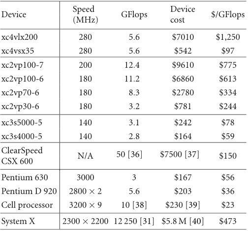
  • As most clusters incorporating FPGAs also include a host processor to handle serial tasks and communication, it is reasonable to assume that the cost analysis in Table 2 favors FPGAs.
  • For Xilinx's double-precision floatingpoint core 16 of these 18-bit multipliers are required [35] for each multiplier, while for the Dou et al. design only nine are needed.
  • While the larger FPGA devices that are prevalent in computational accelerators do not provide a cost benefit for the double-precision floating-point calculations required by the HPC community, historical trends [42] suggest that FPGA performance is improving at a rate faster than that of processors.
  • In both graphs, the latest data point, representing the largest Virtex-4 device, dis-plays worse cost-performance than the previous generation of devices.

2.3. Tools

  • The typical HPC user is a scientist, researcher, or engineer desiring to accelerate some scientific application.
  • Many have noted the requirement of high-level development environments to speed acceptance of FPGA-augmented clusters.
  • These development tools accept a description of the application written in a high level language (HLL) and automate the translation of appropriate sections of code into hardware.
  • Hardware debugging and interfacing still must occur.
  • The use of automatic translation also drives up development costs compared to software implementations.

3.1. Nonstandard data formats

  • The use of IEEE standard floating-point data formats in hardware implementations prevents the user from leveraging an FPGA's fine-grained configurability, effectively reducing an FPGA to a collection of floating-point units with configurable interconnect.
  • Seeing the advantages of customizing the data format to fit the problem, several authors have constructed nonstandard floating-point units.
  • One of the earlier projects demonstrated a 23x speedup on a 2D fast Fourier transform (FFT) through the use of a custom 18-bit floating-point format [44] .
  • For the cost of their PROGRAPE-3 board, estimated at US$ 15,000, it is likely that a 15-node processor cluster could be constructed producing 196 single-precision peak GFLOPS.
  • Many comparisons spend significantly more time optimizing hardware implementations than is spent optimizing software.

3.2. GIMPS benchmark

  • The strength of configurable logic stems from the ability to customize a hardware solution to a specific problem at the bit level.
  • One such application can be found in the great Internet Mersenne prime search [50] .
  • The software used by GIMPS relies heavily on double-precision floating-point FFTs.
  • These memories operated concurrently, two of the buffers feeding the butterfly units while the third exchanged data with the external SDRAM.
  • In spite of the unique all-integer algorithmic approach, the stand-alone FPGA implementation only achieved a speedup of 1.76 compared to a 3.4 GHz Pentium 4 processor.

4. CONCLUSION

  • When comparing HPC architectures many factors must be weighed, including memory and I/O bandwidth, communication latencies, and peak and sustained performance.
  • As the recent focus on commodity processor clusters demonstrates, cost-performance is of paramount importance.
  • In order for FPGAs to gain acceptance within the general HPC community, they must be cost-competitive with traditional processors for the floating-point arithmetic typical in supercomputing applications.
  • The analysis of the costperformance of various current generation FPGAs revealed that only the lower-end devices were cost-competitive with processors for double-precision floating-point matrix multiplications.
  • For lower precision data formats current generation FP-GAs fare much better, being cost-competitive with processors.

Did you find this useful? Give us your feedback
Content maybe subject to copyright    Report

Hindawi Publishing Corporation
EURASIP Journal on Embedded Systems
Volume 2007, Article ID 93652, 8 pages
doi:10.1155/2007/93652
Research Article
Examining the Viability of FPGA Supercomputing
Stephen Craven and Peter Athanas
Bradley Department of Electrical and Computer Engineering, Virginia Polytechnic Institute and State University,
Blacksburg, VA 24061, USA
Received 16 May 2006; Revised 6 October 2006; Accepted 16 November 2006
Recommended by Marco Platzner
For certain applications, custom computational hardware created using field programmable gate arrays (FPGAs) can produce
significant performance improvements over processors, leading some in academia and industry to call for the inclusion of FPGAs
in supercomputing clusters. This paper presents a comparative analysis of FPGAs and traditional processors, focusing on floating-
point performance and procurement costs, revealing economic hurdles in the adoption of FPGAs for general high-performance
computing (HPC).
Copyright © 2007 S. Craven and P. Athanas. This is an open access article distributed under the Creative Commons At tribution
License, which permits unrestricted use, distribution, and reproduction in any medium, provided the original work is properly
cited.
1. INTRODUCTION
Supercomputers have experienced a resurgence, fueled by
government research dollars and the development of low-
cost supercomputing clusters constructed from commodity
PC processors. Recently, interest has arisen in augmenting
these clusters with programmable logic devices, such as FP-
GAs. By tailoring an FPGAs hardware to the specific task at
hand, a custom coprocessor can be created for each HPC ap-
plication.
A wide body of research over two decades has repeat-
edly demonstrated significant performance improvements
for certain classes of applications through hardware accelera-
tion in an FPGA [1]. Applications well suited to acceleration
by FPGAs typically exhibit massive parallelism and small in-
teger or fixed-point data types. Significant performance gains
have been described for gene sequencing [2, 3], digital filter-
ing [4], cryptography [5], network packet filtering [6], target
recognition [7], and pattern matching [8].
ThesesuccesseshaveledSRCComputers[9], DRC Com-
puter Corp. [10], Cray [11], Star bridge Systems [12], and SGI
[13]tooer clusters featuring programmable logic. Cray’s
XD1 architecture, characteristic of many of these systems,
integrates 12 AMD Opteron processors in a chassis with six
large Xilinx Virtex-4 FPGAs. Many systems feature some of
the largest FPGAs in production.
Many HPC applications and benchmarks require double-
precision floating-point arithmetic to support a large dy-
namic range and ensure numerical stability. Floating-point
arithmetic is so prevalent that the benchmarking application
ranking supercomputers, LINPACK, heavily utilizes double-
precision floating-point math. Due to the prevalence of
floating-point arithmetic in HPC applications, research in
academia and industry has focused on floating-point hard-
ware designs [14, 15], libraries [16, 17], and development
tools [18]toeectively perform floating-point math on FP-
GAs. The strong suit of FPGAs, however, is low-precision
fixed-point or integer arithmetic and no current device fam-
ilies contain dedicated floating-point operators though ded-
icated integer multipliers are prevalent. FPGA vendors tai-
lor their products toward their dominant customers, driv-
ing development of architectures proficient at digital sig n al
processing, network applications, and embedded computing.
None of these domains demand floating-point performance.
Published reports comparing FPGA-augmented systems
to software-only implementations generally focus solely on
performance. As a key driver in the adoption of any new tech-
nology is cost, the exclusion of a cost-benefit analysis fails to
capture the true viability of FPGA-based supercomputing. Of
two previous works that do incorporate cost into the analy-
sis, one [19] limits its scope to a single intelligent network
interface design and, while the other [20] presents impres-
sive cost-performance numbers, details and analysis are lack-
ing. Furthermore, many comparisons in literature are inef-
fective, as they compare a highly optimized FPGA floating-
point implementation to nonoptimized software. A much

2 EURASIP Journal on Embedded Systems
Table 1: Published FPGA supercomputing application results.
Application Platform Format Speedup
DGEMM [21] SRC-6 DP 0.9x
Boltzmann [22]
XC2VP70 Float 1x
Dynamics [23]
SRC-6E SP 2x
Dynamics [24]
SRC-6E SP 3x
Dynamics [25]
SRC-6E Float 3.8x
MATPHOT [26]
SRC DP 8.5x
Filtering [27]
SRC-6E Fixed 14x
Translation [28]
SRC-6 Integer 75x
Matching [29]
SRC-6/Cray XD1 Bit 256x/512x
Crypto [30]
SRC-6E Bit 1700x
better benchmark would redesign the algorithm to play to
the FPGAs strengths, comparing the designs performance to
that of an optimized program.
The key contributions of this paper are the addition of an
economic analysis to a discussion of FPGA supercomputing
projects and the presentation of an eective benchmark for
comparing FPGAs and processors on an equal footing. A sur-
vey of current research, along with a cost-performance anal-
ysis of FPGA floating-point implementations, is presented in
Section 2. Section 3 describes alternatives to floating-point
implementations in FPGAs, presenting a balanced bench-
mark for comparing FPGAs to processors. Finally, conclu-
sions are presented in Section 4.
2. FPGA SUPERCOMPUTING TRENDS
This sect ion presents an overview of the use of FPGAs in su-
percomputers, analyzing the reported performance enhance-
ments from a cost perspective.
2.1. HPC implementations
The availability of high-performance clusters incorporating
FPGAs has prompted eorts to explore acceleration of HPC
applications. While not an exhaustive list, Table 1 provides
a survey of recent representative applications. The SRC-6
and 6E combine two Xeon or Pentium processors with two
large Virtex-II or Virtex-II Pro FPGAs. The Cray XD1 places
a Virtex-4 FPGA on a special interconnect system for low-
latency communication with the host Opteron processors.
In the table, the applications are listed by performance.
The abbreviations SP and DP refer to single-precision
and double-precision floating point, respectively. While the
speedups provided in the table are not normalized to a com-
mon processor, a trend is clearly visible. The top six examples
all incorporate floating-point arithmetic and fare worse than
the applications that utilize small data widths.
With no cost information regarding the SRC-6 or Cray
XD1 available to the authors a thorough cost-performance
analysis is not possible. However, as the cost of the FPGA ac-
celeration hardware in these machines alone likely is on the
order of US$10 000 or more, it is likely that the floating-point
examples may loose some of their appeal when compared to
processors on a cost-eective basis. The obser ved speedups
of 75–1700 for integer and bit-level operations, on the other
hand, would likely be very beneficial from a cost perspective.
2.2. Theoretical floating-point performance
FPGA designs may suer significant performance penalties
due to memory and I/O bottlenecks. To understand the po-
tential of FPGAs in the absence of b ottlenecks, it is instructive
to consider the theoretical maximum floating-point perfor-
mance of an FPGA.
Traditional processors, with a fixed data path width of
32 or 64 bits, provide no incentive to explore reduced pre-
cision formats. While FPGAs permit data path width cus-
tomization, some in the HPC community are loath to utilize
a nonstandard format owing to verification and portability
diculties. This principle is at the heart of the Top500 List
of fastest supercomputers [31], where ranked machines must
exactly reproduce valid results w hen running the LINPACK
benchmarks. Many applications also require the full dynamic
range of the double-precision format to ensure numeric sta-
bility.
Due to the prevalence of IEEE standard floating-point
in a wide range of applications, several researchers have de-
signed IEEE 754 compliant floating-point accelerator cores
constructed out of the Xilinx Virtex-II Pro FPGAs config-
urable logic and dedicated integer multipliers [3234]. Dou
et al. published one of the highest performance benchmarks
of 15.6 GFLOPS by placing 39 floating-point processing el-
ements on a theoretical Xilinx XC2VP125 FPGA [14]. Inter-
polating their results for the largest production Xilinx Virtex-
II Pro device, the XC2VP100, produces 12.4 GFLOPS, com-
pared to the peak 6.4 GFLOPS achievable for a 3.2 GHz Intel
Pentium processor. Assuming that the Pentium can sustain
50% of its peak, the FPGA outperforms the processor by a
factor of four for matrix multiplication.
Dou et al.s design is comprised of a linear array of MAC
elements, linked to a host processor providing memory ac-
cess. The design is pipelined to a depth of 12, permitting op-
eration at a frequency up to 200 MHz. This architecture en-
ables high computational density by simplifying routing and
control, at the requirement of a host controller. Since the re-
sults of Dou et al. are superior to other published results, and
even Xilinx’s floating-point cores, they are taken as a n abso-
lute upper limit on FPGAs double-precision floating-point
performance. Performance in any deployed system would be
lower because of the addition of interface logic.
Table 2 extrapolates Dou et al.s performance results for
other FPGA device families. Given the similar configurable
logic architectures between the dierent Xilinx families, it
has been assumed that D ou et al.s requirements of 1419
logic slices and nine dedicated multipliers hold for all fam-
ilies. While the slice requirements may be less for the Virtex-
4 family, owing to the inclusion of an MAC function with
the dedicated multipliers, as all considered Virtex-4 imple-
mentations were multiplier limited the overestimate in re-
quired slices does not aect the results. The clock frequency

S. Craven and P. Athanas 3
Table 2: Double-precision floating-point multiply accumulate
cost-performance in US dollars.
Device
Speed
(MHz)
GFlops
Device
cost
$/GFlops
xc4vlx200 280 5.6 $7010 $1,250
xc4vsx35
280 5.6 $542 $97
xc2vp100-7 200 12.4 $9610 $775
xc2vp100-6
180 11.2 $6860 $613
xc2vp70-6
180 8.3 $2780 $334
xc2vp30-6
180 3.2 $781 $244
xc3s5000-5 140 3.1 $242 $78
xc3s4000-5
140 2.8 $164 $59
ClearSpeed
CSX 600
N/A
50 [36] $7500 [37]
$150
Pentium 630 3000 3 $167 $56
Pentium D 920
2800 × 2 5.6 $203 $36
Cell processor
3200 × 910[38] $230 [39] $23
System X 2300 × 2200 12 250 [31] $5.8 M [40] $473
has been scaled by a factor obtained by averaging the perfor-
mance dierential of Xilinx’s double-precision floating-point
multiplier and adder cores [35] across the dierent families.
For comparison purposes, several commercial processors
have been included in the list. The peak performance for each
processor was reduced by 50%, taking into account compiler
and system ineciencies, permitting a fairer comparison as
FPGAs designs typically sustain a much higher percentage of
their peak performance than processors. This 50% perfor-
mance penalty is in line with the sustained performance seen
in the Top500 List’s LINPACK benchmark [31]. In the table,
FPGAs are assumed to sustain their peak performance.
As can be seen from the table, FPGA double-precision
floating-point performance is noticeably higher than for tra-
ditional Intel processors; however, considering the cost of
this performance processors fare better, with the worst pro-
cessor beating the best FPGA. In particular, Sony’s Cell pro-
cessor is more than two times cheaper per GFLOPS than the
best FPGA. The results indicate that the current generation of
larger FPGAs found on many FPGA-augmented HPC clus-
ters are far from cost competitive with the current genera-
tion of processors for double-precision floating-point tasks
typical of supercomputing applications.
With two exceptions, ClearSpeed and System X, all costs
in Table 2 only cover the price of the device not including
other components (motherboard, memory, network, etc.)
that are necessary to produce a functioning supercomputer.
It is also assumed here that operational costs are equiva-
lent. These additional costs are nonnegligible and, while the
FPGA accelerators would also incur additional costs for cir-
cuit board and components, it is likely that the cost of com-
ponents to create a functioning HPC node from a processor,
even factoring in economies of scale, would be larger than for
creating an accelerator plug-in from an FPGA. However, as
most clusters incorporating FPGAs also include a host pro-
cessor to handle serial tasks and communication, it is reason-
able to assume that the cost analysis in Ta ble 2 favors FPGAs.
To place the additional component costs in perspec-
tive, the cost-performance for Virginia Techs System X su-
percomputing cluster has been included [41]. Constructed
from 1100 dual core Apple XServe nodes, the supercom-
puter, including the cost of all components, cost US$473 per
GFLOPS. Several of the larger FPGAs cost more per GFLOPS
even without the memory, boards, and assembly required to
create a functional accelerator.
As the dedicated integer multipliers included by Xilinx,
the largest configurable logic manufacturer, are only 18-bits
wide, se veral multipliers must be combined to produce the
52-bit multiplication needed for double-precision floating-
point multiplication. For Xilinx’s double-precision floating-
point core 16 of these 18-bit multipliers are required [35]
for each multiplier, w hile for the Dou et al. design only nine
are needed. For many FPGA dev ice families the high multi-
plier requirement limits the number of floating-point multi-
pliers that may be placed on the dev ice. For example, while
31 of Dous MAC units may be placed on an XC2VP100, the
largest Virtex-II Pro device, the lack of sucient dedicated
multipliers permits only 10 to be placed on the largest Xilinx
FPGA, an XC4VLX200. If this dev ice was solely used as a ma-
trix multiplication accelerator, as in Dous work, over 80% of
the device would be unused. Of course this idle configurable
logic could be used to implement additional multipliers, at a
significant p erformance penalty.
While the larger FPGA devices that are prevalent in com-
putational accelerators do not provide a cost benefit for the
double-precision floating-point calculations required by the
HPC community, historical trends [42] suggest that FPGA
performance is improving at a rate faster than that of pro-
cessors. The question is then asked, when, if ever, will FPGAs
overtake processors in cost performance?
As has been noted by some, the cost of the largest cutt-
ing-edge FPGA remains roughly constant over time, while
performance and size improve. A first-order estimate of US$
8,000 has been made for the cost of the largest and newest
FPGA—an estimate supported by the cost of the largest
Virtex-II Pro and Virtex-4 devices. Furthermore, it is as-
sumed that the cost of a processor remains constant at
US$500 over time as well. While these estimates are some-
what misleading, as these costs certainly do vary over time,
the variability in the cost of computing devices between
generations is much less than the increase in performance.
The comparison further assumes, as before, that processors
can sustain 50% of their peak floating-point performance
while FPGAs sustain 100%. Whenever possible, estimates
were rounded to favor FPGAs.
Two sources of data were used for performance extrap-
olation to increase the validity of the results. The work of
Dou et al. [14], representing the fastest double-precision
floating-point MAC design, was extrapolated to the largest
parts in several Xilinx device families. Additional data was
obtained by extrapolating the results of Underwood’s histor-
ical analysis [42] to include the Virtex-4 family. Underwood’s

4 EURASIP Journal on Embedded Systems
2000 2002 2004 2006 2008 2010
10
100
1000
10000
Cost/GFLOPS ($)
Yea r
FPGAs
Processors
Extrapolation FPGA w/o Virtex-4
Extrapolation FPGA
Extrapolation processor
(a)
2000 2002 2004 2006 2008 2010
10
100
1000
10000
Cost/GFLOPS ($)
Yea r
FPGAs
Processors
Extrapolation FPGA w/o Virtex-4
Extrapolation FPGA
Extrapolation processor
(b)
Figure 1: Extrapolated double-precision floating-point MAC cost-
performance, in US dollars, for: (a) Underwood design and (b) Dou
et al. desig n.
data came from his IEEE standard floating-point designs
pipelined, depending on the device, to a maximum depth of
34. The results are shown in Figure 1(a) for the Underwood
data and Figure 1(b) for Dou et al.
An additional data point exists for the Underwood graph
as his work included results for the Virtex-E FPGAs. The
Dou et al. design is higher performance and smaller, in terms
of slices, than Underwood’s design. In both graphs, the lat-
est data point, representing the largest Virtex-4 device, dis-
plays worse cost-performance than the previous generation
of devices. This is due to the shortage of dedicated multipli-
ers on the larger Virtex-4 devices. The Virtex-4 architecture
is comprised of three subfamilies: the LX, SX, and FX. The
Virtex-4 subfamily with the largest devices, by far, is the LX
and it is these devices that are found in FPGA-augmented
HPC nodes. However, the LX subfamily is focused on logic
density, trading most of the dedicated multipliers found in
the smaller SX subfamily for configurable logic. This signifi-
cantly reduces the floating-point multiplication performance
of the larger Virtex-4 devices.
As the graphs illustrate, if this trend towards logic-centric
large FPGAs continues it is u nlikely that the largest FPGAs
will be cost eective compared to processors anytime soon,
if ever. However, as preliminary data on the next-generation
Virtex-5 suggests that the relatively poor floating-point per-
formance of the Virtex-4 is an aberration and not indica-
tive of a trend in FPGA architectures, it seems reasonable
to reconsider the results excluding the Virtex-4 data points.
Figure 1 trend lines labeled “FPGA extr apolation w/o Virtex-
4” exclude these potential misleading data points.
When the Virtex-4 data is ignored, the cost-performance
of FPGAs for double-precision floating-point matrix multi-
plication improves at a rate greater than that for processors.
While there is always a danger from drawing conclusions
from a small data set, both the Dou et al. and Underwood
design results point to a crossover point sometime around
2009 to 2012 when the largest FPGA devices, like those typ-
ically found in commercial FPGA-augmented HPC clusters,
will be cost eectively compared to processors for double-
precision floating-point calculations.
2.3. Tools
The typical HPC user is a scientist, researcher, or engineer
desiring to accelerate some scientific application. These users
are generally acquainted with a programming language ap-
propriate to their fields (C, FORTAN, MATLAB, etc.) but
have little, if any, hardware design knowledge. Many have
noted the requirement of high-level development environ-
ments to speed acceptance of FPGA-augmented clusters.
These de velopment tools accept a description of the appli-
cation written in a high level language (HLL) and automate
the translation of appropriate sections of code into hardware.
Several companies market HLL-to-gates synthesizers to the
HPC community, including impulse accelerated technolo-
gies, Celoxica, and SRC.
The state of these tools, however, as noted by some [43],
does not remove the need for dedicated hardware expertise.
Hardware debugging and interfacing still must occur. The
use of automatic translation also drives up development costs
compared to software implementations. C compilers and de-
buggers are free. Electronic design automation tools, on the
other hand, may require expensive yearly licenses. Further-
more, the added ineciencies of translating an inherently
sequential high-level description into a parallel hardware im-
plementation eat into the performance of hardware accelera-
tors.

S. Craven and P. Athanas 5
3. FLOATING-POINT ALTERNATIVES
3.1. Nonstandard data formats
The use of IEEE standard floating-point data formats in
hardware implementations prevents the user from le verag-
ing an FPGAs fine-g rained configurability, eectively reduc-
ing an FPGA to a collection of floating-point units with con-
figurable interconnect. Seeing the advantages of customizing
the data format to fit the problem, several authors have con-
structed nonstandard floating-point units.
One of the earlier projects demonstr ated a 23x speedup
on a 2D fast Fourier transform (FFT) through the use of a
custom 18-bit oating-point form at [44]. More recent work
has focused on parameterizible libraries of floating-point
units that can be tailored to the task at hand [4547]. By us-
ing a custom floating-point format sized to match the width
of the FPGAs internal integer multipliers, a speedup of 44
was achieved by Nakasato and Hamada for a hydrodynamics
simulation [48] using four large FPGAs.
Nakasato and Hamadas 38 GFLOPS of performance is
impressive, even from a cost-performance standpoint. For
the cost of their PROGRAPE-3 board, estimated at US$
15,000, it is likely that a 15-node processor cluster could be
constructed producing 196 single-precision peak GFLOPS.
Even in the unlikely scenario that this cluster could sus-
tain the same 10% of peak performance obtained by Naka-
sato and Hamadas for their software implementation, the
PROGRAPE-3 design would still achieve a 2x speedup.
As in many FPGA to CPU comparisons, it is likely that
the analysis unfairly favors the FPGA solution. Many com-
parisons spend significantly more time optimizing hardware
implementations than is spent optimizing software. Signif-
icant compiler ineciencies exist for common HPC func-
tions [49], with some hand-coded functions outperform-
ing the compiler by many times. It is possible that Nakasato
and Hamadas speedup would be significantly reduced, and
perhaps e liminated on a cost-performance basis, if equal
eort was applied to optimizing software at the assembly
level. However, to permit their design to be more cost-
competitive, even against ecient software implementations,
smaller more cost-eective FPGAs could be used.
3.2. GIMPS benchmark
The strength of configurable logic stems from the ability to
customize a hardware solution to a specific problem at the bit
level. The previously presented works implemented coarse-
grained floating-point units inside an FPGA for a wide range
of HPC applications. For certain applications the full flexibil-
ity of configurable logic can be leveraged to create a custom
solution to a specific problem, utilizing data ty pes that play
to the FPGAs strengths—integer arithmetic.
One such application can be found in the great Inter-
net Mersenne prime search (GIMPS) [50]. The software used
by GIMPS relies heavily on double-precision floating-point
FFTs. Through a careful analysis of the problem, an all-
integer solution is possible that improves FPGA performance
by a factor of two and avoids the inaccuracies inherit in
floating-point math.
The largest known prime numbers are Mersenne pri-
mes—prime numbers of the form 2
q
1, where q is also
prime. The distributed computing project GIMPS was cre-
ated to identify large Mersenne primes and a reward of
US$100,000 has been issued for the first person to identify
a prime number with greater than 10 million digits. The al-
gorithm used by GIMPS, the Lucas-Lehmer test, is iterative,
repeatedly performing modular squaring .
One of the most ecient multiplication algorithms for
large integers utilizes the FFT, treating the number being
squared as a long sequence of smaller numbers. The linear
convolution of this sequence with itself performs the squar-
ing. As linear convolution in the time domain is equivalent
to multiplication in the frequency domain, the FFT of the se-
quence is taken and the resulting frequency domain sequence
is squared elementwise before being brought back into the
time domain. Floating-point arithmetic is used to meet the
strict precision requirements across the time and frequency
domains. The software used by GIMPS has been optimized
at the assembly level for maximum performance on Pentium
processors, making this application an eec tive benchmark
of relative processor floating-point performance.
Previous work focused on an FPGA hardware implemen-
tation of the GIMPS algorithm to compare FPGA and pro-
cessor floating-point performance [51]. Performing a tradi-
tional port of the algorithm from software to hardware in-
volves the creation of a floating-point FFT on the FPGA.
On an XC2VP100, the largest Virtex-II Pro, 12 near-double-
precision complex multipliers could be created from the 444
dedicated integer multipliers. Such a design with pipelining
performs a single iteration of the Lucas-Lehmer test in 3.7
million clock cycles.
To leverage the advantages of a configurable architec-
ture an all-integer number theoretical transform was con-
sidered. In particular, the irrational base discrete weighted
transform (IBDWT) can be used to perform integer convo-
lution, serving the exact same purpose as the floating-point
FFT in the Lucas-Lehmer test. In the IBDWT, all arithmetic is
performed modulo a special prime number. Normally mod-
ulo arithmetic is a demanding operation requiring many cy-
cles of latency, but by careful selection of this pr ime num-
ber the reduction can be performed by simple additions and
shifting [51]. The resulting all-integer implementation incor-
porates two 8-point butterfly structures constructed with 24-
64-bit integer multipliers and pipelined to a depth of 10. A
single iteration of Lucas-Lehmer requires 1.7 million clock
cycles, a more than two-fold improvement over the floating-
point design.
The final GIMPS accelerator, shown in Figure 2 imple-
mented in the largest Virtex-II Pro FPGA, consisted of two
butterflies fed by reorder caches constructed from the inter-
nal memories. To prevent a memory bottleneck, the design
assumed four independent banks of double data rate (DDR)
SDRAM. Three sets of reorder buers were created out of
the dedicated block memories on the device. These mem-
ories operated concurrently, two of the buers feeding the
butterfly units while the third exchanged data with the ex-
ternal SDRAM. The final design could be clocked at 80 MHz

Citations
More filters
Proceedings ArticleDOI
31 Aug 2009
TL;DR: The performance of the memory copies and GEMM subroutines that are crucial to port the computational chemistry algorithms to the GPU clusters are studied and are compared with that of the BLAS routines from the Intel Math Kernel Library (MKL) to understand the computational trade-offs.
Abstract: Commodity clusters augmented with application accelerators are evolving as competitive high performance computing systems. The Graphical Processing Unit (GPU) with a very high arithmetic density and performance per price ratio is a good platform for the scientific application acceleration. In addition to the interconnect bottlenecks among the cluster compute nodes, the cost of memory copies between the host and the GPU device have to be carefully amortized to improve the overall efficiency of the application. Scientific applications also rely on efficient implementation of the Basic Linear Algebra Subroutines (BLAS), among which the General Matrix Multiply (GEMM) is considered as the workhorse subroutine. In this paper, we study the performance of the memory copies and GEMM subroutines that are crucial to port the computational chemistry algorithms to the GPU clusters. To that end, a benchmark based on the NetPIPE [1] framework is developed to evaluate the latency and bandwidth of the memory copies between the host and the GPU device. The performance of the single and double precision GEMM subroutines from the NVIDIA CUBLAS 2.0 library are studied. The results have been compared with that of the BLAS routines from the Intel Math Kernel Library (MKL) to understand the computational trade-offs. The test bed is a Intel Xeon cluster equipped with NVIDIA Tesla GPUs.

14 citations


Cites background from "Examining the viability of FPGA sup..."

  • ...These insights would also in a a broader scope be useful to develop a unified framework under which a comparative analysis can be made among clusters deployed with other types of application accelerators such as PowerXCell 8i [9] and Field Programmable Gate Arrays (FPGA) [10]....

    [...]

Proceedings ArticleDOI
09 Dec 2009
TL;DR: It is shown that, for algorithms with highly similar traversals, the traversal cache framework achieves approximately linear kernel speedup with additional area, thus eliminating the memory bandwidth bottleneck commonly associated with FPGAs.
Abstract: Numerous studies have shown that field-programmable gate arrays (FPGAs) often achieve large speedups compared to microprocessors. However, one significant limitation of FPGAs that has prevented their use on important applications is the requirement for regular memory access patterns. Traversal caches were previously introduced to improve the performance of FPGA implementations of algorithms with irregular memory access patterns, especially those traversing pointer-based data structures. However, a significant limitation of previous traversal caches is that speedup was limited to traversals repeated frequently over time, thus preventing speedup for algorithms without repetition, even if the similarity between traversals was large. This paper presents a new framework that extends traversal caches to enable performance improvements in such cases and provides additional improvements through reduced memory accesses and parallel processing of multiple traversals. Most importantly, we show that, for algorithms with highly similar traversals, the traversal cache framework achieves approximately linear kernel speedup with additional area, thus eliminating the memory bandwidth bottleneck commonly associated with FPGAs. We evaluate the framework using a Barnes-Hut n-body simulation case study, showing application speedups ranging from 12x to 13.5x on a Virtex4 LX100 with projected speedups as high as 40x on today’s largest FPGAs.

14 citations


Cites background from "Examining the viability of FPGA sup..."

  • ...Keywords-FPGA, traversal cache, pointers, speedup I. INTRODUCTION Much previous work has shown that field-programmable gate arrays (FPGAs) can achieve order of magnitude speedups compared to microprocessors for many important embedded and scientific computing applications [3][4][9]....

    [...]

Dissertation
01 Jul 2013
TL;DR: The developed solution in this thesis is named as R3TOS, which stands for Reliable Reconfigurable Real-Time Operating System, which defines a flexible infrastructure for reliably executing reconfigurable hardware-based applications under real-time constraints.
Abstract: Twenty-first century Field-Programmable Gate Arrays (FPGAs) are no longer used for implementing simple “glue logic” functions. They have become complex arrays of reconfigurable logic resources and memories as well as highly optimised functional blocks, capable of implementing large systems on a single chip. Moreover, Dynamic Partial Reconfiguration (DPR) capability permits to adjust some logic resources on the chip at runtime, whilst the rest are still performing active computations. During the last few years, DPR has become a hot research topic with the objective of building more reliable, efficient and powerful electronic systems. For instance, DPR can be used to mitigate spontaneously occurring bit upsets provoked by radiation, or to jiggle around the FPGA resources which progressively get damaged as the silicon ages. Moreover, DPR is the enabling technology for a new computing paradigm which combines computation in time and space. In Reconfigurable Computing (RC), a battery of computation-specific circuits (“hardware tasks”) are swapped in and out of the FPGA on demand to hold a continuous stream of input operands, computation and output results. Multitasking, adaptation and specialisation are key properties in RC, as multiple swappable tasks can run concurrently at different positions on chip, each with custom data-paths for efficient execution of specific computations. As a result, considerable computational throughput can be achieved even at low clock frequencies. However, DPR penetration in the commercial market is still testimonial, mainly due to the lack of suitable high-level design tools to exploit this technology. Indeed, currently, special skills are required to successfully develop a dynamically reconfigurable application. In light of the above, this thesis aims at bridging the gap between high-level application and low-level DPR technology. Its main objective is to develop Operating System (OS)-like support for high-level software-centric application developers in order to exploit the benefits brought about by DPR technology, without having to deal with the complex low-level hardware details. The developed solution in this thesis is named as R3TOS, which stands for Reliable Reconfigurable Real-Time Operating System. R3TOS defines a flexible infrastructure for reliably executing reconfigurable hardware-based applications under real-time constraints. In R3TOS, the hardware tasks are scheduled in order to meet their computation deadlines and allocated to non-damaged resources, keeping the system fault-free at all times. In addition, R3TOS envisages a computing framework whereby both hardware and software tasks coexist in a seamless manner, allowing the user to access the advanced computation capabilities of modern reconfigurable hardware from a software “look and feel” environment. This thesis covers all of the design and implementation aspects of R3TOS. The thesis proposes a novel EDF-based scheduling algorithm, two novel task allocation heuristics (EAC and EVC) and a novel task allocation strategy…

11 citations

Book ChapterDOI
21 Jul 2008
TL;DR: A model is developed that can assist designers at the system-level DSE stage to explore the utilization of the reconfigurable resources and evaluate the relative impact of certain design choices and can be used to explore various design parameters by evaluating the system performance for different application-to-architecture mappings.
Abstract: One of the major challenges of designing heterogeneous reconfigurable systems is to obtain the maximum system performance with efficient utilization of the reconfigurable logic resources. To accomplish this, it is essential to perform design space exploration (DSE) at the early design stages. System-level simulation is used to estimate the performance of the system and to make early decisions of various design parameters in order to obtain an optimal system that satisfies the given constraints. Towards this goal, in this paper, we develop a model, which can assist designers at the system-level DSE stage to explore the utilization of the reconfigurable resources and evaluate the relative impact of certain design choices. A case study of a real application shows that the model can be used to explore various design parameters by evaluating the system performance for different application-to-architecture mappings.

10 citations

Book ChapterDOI
23 Mar 2012
TL;DR: Computer Vision systems are experiencing a large increase in both range of applications and market sales, and new algorithms provide more advanced and comprehensive analysis of the images, expanding the set of tools to implement applications.
Abstract: Computer Vision systems are experiencing a large increase in both range of applications and market sales (BCC Research, 2010) From industry to entertainment, Computer Vision systems are becoming more and more relevant The research community is making a big effort to develop systems able to handle complex scenes focusing on the accuracy and the robustness of the results New algorithms provide more advanced and comprehensive analysis of the images, expanding the set of tools to implement applications (Szeliski, 2010)

9 citations


Cites methods from "Examining the viability of FPGA sup..."

  • ...FPGAs are widely employed as co-processors in personal computers such as GPUs or as accelerators in specific purpose devices as high-capacity network systems (Djordjevic et al., 2009) or high-performance computing (Craven & Athanas, 2007)....

    [...]

References
More filters
Journal ArticleDOI
TL;DR: The hardware aspects of reconfigurable computing machines, from single chip architectures to multi-chip systems, including internal structures and external coupling are explored, and the software that targets these machines is focused on.
Abstract: Due to its potential to greatly accelerate a wide variety of applications, reconfigurable computing has become a subject of a great deal of research. Its key feature is the ability to perform computations in hardware to increase performance, while retaining much of the flexibility of a software solution. In this survey, we explore the hardware aspects of reconfigurable computing machines, from single chip architectures to multi-chip systems, including internal structures and external coupling. We also focus on the software that targets these machines, such as compilation tools that map high-level algorithms directly to the reconfigurable substrate. Finally, we consider the issues involved in run-time reconfigurable systems, which reuse the configurable hardware during program execution.

1,666 citations


"Examining the viability of FPGA sup..." refers background in this paper

  • ...A wide body of research over two decades has repeatedly demonstrated significant performance improvements for certain classes of applications through hardware acceleration in an FPGA [1]....

    [...]

Journal ArticleDOI
TL;DR: It is shown that the Cell/B.E.E., or Cell Broadband Engine, processor can outperform other modern processors by approximately an order of magnitude and by even more in some cases.
Abstract: The Cell Broadband Engine™ (Cell/B.E.) processor is the first implementation of the Cell Broadband Engine Architecture (CBEA), developed jointly by Sony, Toshiba, and IBM. In addition to use of the Cell/B.E. processor in the Sony Computer Entertainment PLAYSTATION® 3 system, there is much interest in using it for workstations, media-rich electronics devices, and video and image processing systems. The Cell/B.E. processor includes one PowerPC® processor element (PPE) and eight synergistic processor elements (SPEs). The CBEA is designed to be well suited for a wide variety of programming models, and it allows for partitioning of work between the PPE and the eight SPEs. In this paper we show that the Cell/B.E. processor can outperform other modern processors by approximately an order of magnitude and by even more in some cases.

401 citations


Additional excerpts

  • ...Cell processor 3200 × 9 10 [38] $230 [39] $23 System X 2300 × 2200 12 250 [31] $5....

    [...]

Journal ArticleDOI
01 May 2001
TL;DR: A survey of academic research and commercial development in reconfigurable computing for DSP systems over the past fifteen years is presented in this article, with a focus on the application domain of digital signal processing.
Abstract: Steady advances in VLSI technology and design tools have extensively expanded the application domain of digital signal processing over the past decade. While application-specific integrated circuits (ASICs) and programmable digital signal processors (PDSPs) remain the implementation mechanisms of choice for many DSP applications, increasingly new system implementations based on reconfigurable computing are being considered. These flexible platforms, which offer the functional efficiency of hardware and the programmability of software, are quickly maturing as the logic capacity of programmable devices follows Moore's Law and advanced automated design techniques become available. As initial reconfigurable technologies have emerged, new academic and commercial efforts have been initiated to support power optimization, cost reduction, and enhanced run-time performance. This paper presents a survey of academic research and commercial development in reconfigurable computing for DSP systems over the past fifteen years. This work is placed in the context of other available DSP implementation media including ASICs and PDSPs to fully document the range of design choices available to system engineers. It is shown that while contemporary reconfigurable computing can be applied to a variety of DSP applications including video, audio, speech, and control, much work remains to realize its full potential. While individual implementations of PDSP, ASIC, and reconfigurable resources each offer distinct advantages, it is likely that integrated combinations of these technologies will provide more complete solutions.

390 citations

Proceedings ArticleDOI
22 Feb 2004
TL;DR: This paper examines the impact of Moore's Law on the peak floating-point performance of FPGAs and results show that peak FPGA floating- point performance is growing significantly faster than peak CPU performance for a CPU.
Abstract: Moore's Law states that the number of transistors on a device doubles every two years; however, it is often (mis)quoted based on its impact on CPU performance. This important corollary of Moore's Law states that improved clock frequency plus improved architecture yields a doubling of CPU performance every 18 months. This paper examines the impact of Moore's Law on the peak floating-point performance of FPGAs. Performance trends for individual operations are analyzed as well as the performance trend of a common instruction mix (multiply accumulate). The important result is that peak FPGA floating-point performance is growing significantly faster than peak floating-point performance for a CPU.

341 citations


"Examining the viability of FPGA sup..." refers background or methods in this paper

  • ...Additional data was obtained by extrapolating the results of Underwood’s historical analysis [25] to include the Virtex 4 family....

    [...]

  • ...Extrapolated Cost-Performance Comparison While the larger FPGA devices that are prevalent in computational accelerators do not provide a cost benefit for the double precision floating-point calculations required by the HPC community, historical trends [25] suggest that FPGA performance is improving at a rate faster than that of processors....

    [...]

Proceedings ArticleDOI
20 Feb 2005
TL;DR: A 64-bit ANSI/IEEE Std 754-1985 floating point design of a hardware matrix multiplier optimized for FPGA implementations and implement a scalable linear array of processing elements (PE) supporting the proposed algorithm in the Xilinx Virtex II Pro technology.
Abstract: We introduce a 64-bit ANSI/IEEE Std 754-1985 floating point design of a hardware matrix multiplier optimized for FPGA implementations. A general block matrix multiplication algorithm, applicable for an arbitrary matrix size is proposed. The algorithm potentially enables optimum performance by exploiting the data locality and reusability incurred by the general matrix multiplication scheme and considering the limitations of the I/O bandwidth and the local storage volume. We implement a scalable linear array of processing elements (PE) supporting the proposed algorithm in the Xilinx Virtex II Pro technology. Synthesis results confirm a superior performance-area ratio compared to related recent works. Assuming the same FPGA chip, the same amount of local memory, and the same I/O bandwidth, our design outperforms related proposals by at least 1.7X and up to 18X consuming the least reconfigurable resources. A total of 39 PEs can be integrated into the xc2vp125-7 FPGA, reaching performance of, e.g., 15.6 GFLOPS with 1600 KB local memory and 400 MB/s external memory bandwidth.

224 citations


"Examining the viability of FPGA sup..." refers background or methods in this paper

  • ...6 GFLOPS by placing 39 floating-point processing elements on a theoretical Xilinx XC2VP125 FPGA [14]....

    [...]

  • ...Due to the prevalence of floating-point arithmetic in HPC applications, research in academia and industry has focused on floating-point hardware designs [14, 15], libraries [16, 17], and development tools [18] to effectively perform floating-point math on FPGAs....

    [...]

  • ...[14], representing the fastest double-precision floating-point MAC design, was extrapolated to the largest parts in several Xilinx device families....

    [...]

  • ...Dou et al. published one of the highest performance benchmarks of 15.6 GFLOPS by placing 39 floating-point processing elements on a theoretical Xilinx XC2VP125 FPGA [14]....

    [...]

Frequently Asked Questions (16)
Q1. What are the contributions in "Examining the viability of fpga supercomputing" ?

This paper presents a comparative analysis of FPGAs and traditional processors, focusing on floatingpoint performance and procurement costs, revealing economic hurdles in the adoption of FPGAs for general high-performance computing ( HPC ). 

The strong suit of FPGAs, however, is low-precision fixed-point or integer arithmetic and no current device families contain dedicated floating-point operators though dedicated integer multipliers are prevalent. 

One of the most efficient multiplication algorithms for large integers utilizes the FFT, treating the number being squared as a long sequence of smaller numbers. 

When comparing HPC architectures many factors must be weighed, including memory and I/O bandwidth, communication latencies, and peak and sustained performance. 

Many HPC applications and benchmarks require doubleprecision floating-point arithmetic to support a large dy-namic range and ensure numerical stability. 

to permit their design to be more costcompetitive, even against efficient software implementations, smaller more cost-effective FPGAs could be used. 

The distributed computing project GIMPS was created to identify large Mersenne primes and a reward of US$100,000 has been issued for the first person to identify a prime number with greater than 10 million digits. 

Floating-point arithmetic is so prevalent that the benchmarking application ranking supercomputers, LINPACK, heavily utilizes doubleprecision floating-point math. 

Due to the prevalence of floating-point arithmetic in HPC applications, research in academia and industry has focused on floating-point hardware designs [14, 15], libraries [16, 17], and development tools [18] to effectively perform floating-point math on FPGAs. 

For Xilinx’s double-precision floatingpoint core 16 of these 18-bit multipliers are required [35] for each multiplier, while for the Dou et al. design only nine are needed. 

A slightly reworked implementation, designed as an FFT accelerator with all serial functions implemented on an attached processor, could achieve a speedup of 2.6 compared to a processor alone. 

The availability of high-performance clusters incorporating FPGAs has prompted efforts to explore acceleration of HPC applications. 

The key contributions of this paper are the addition of an economic analysis to a discussion of FPGA supercomputing projects and the presentation of an effective benchmark for comparing FPGAs and processors on an equal footing. 

Performing a traditional port of the algorithm from software to hardware involves the creation of a floating-point FFT on the FPGA. 

In spite of the unique all-integer algorithmic approach, the stand-alone FPGA implementation only achieved a speedup of 1.76 compared to a 3.4 GHz Pentium 4 processor. 

While there is always a danger from drawing conclusions from a small data set, both the Dou et al. and Underwood design results point to a crossover point sometime around 2009 to 2012 when the largest FPGA devices, like those typically found in commercial FPGA-augmented HPC clusters, will be cost effectively compared to processors for doubleprecision floating-point calculations.