Memristor-based memory
Summary (3 min read)
1. Introduction
- Memristors (memory resistors) offer a promising alternative to conventional memory devices.
- Since the first reported use of the memristor, it received a significant of attention in the research community.
- The authors analysis is based on simulations for different memory array sizes, data sets, and architectures using the models presented in [17].
- Moreover, the authors study the effect of the aspect ratio of the memory array on the sneak paths.
2. Memristor-Based Memory
- Memristor-based memories are fabricated as a high-density crossbar architecture.
- Memristor devices are located at each intersection between two bars, as shown in Fig.
- Table 1 shows a detailed comparison between memristorbased memory, traditional memories, and other emerging memories.
- HP Labs are currently reporting a fast switching time of less than 2ns [38].
- Recently, Elpida Memory Inc., reported the development of a high-speed non-volatile resistance memory [39].
2.1. Writing Operation
- Data are stored in the memristor in the form of its resistance value, where each of the limiting resistances.
- Ro f f and Ron are the maximum and minimum resistances of the device, respectively.
- Writing one of these values is simply done by passing current through the cell of interest until the memristor’s resistance saturates.
- Even this simple writing operation could consume considerable of energy, depending on the values of the memristor’s resistances.
2.3. Multilevel Memory
- Multilevel memory is one promising application for the memristor device.
- Using such a technique would enormously increase the density of memristor-based memory, but would also reduce the noise margin significantly.
- The current proposed techniques for building binary memristor-based memory suffer from many problems that could be fatal for the multilevel memory.
- Some researchers believe 1M is insufficient for building multilevel memory, and that 1M1T (one memristor and one transistor) or 1M1D (one memristor and one diode) are needed [42].
- The authors believe that addressing the current challenges facing the binary memristor-based memory will directly solve the multilevel memory problems.
3. Sneak Paths Analysis
- Sneak paths are undesired paths for current, parallel to the intended path.
- The sets are selected to reflect both the worst and best cases for the memory content.
- The simulation result is independent of the location of the cell in the array if the authors neglect the rows’ and columns’ pad resistances.
- In conventional CMOS circuits, there are two regions defined for accepted values of ONEs and ZEROs [43], as shown in Fig.
- For a given data pattern stored in the memory, the difference between voltages values representing ONE and ZERO at the target cell is a perfect measure for the sneak-path effect.
3.1. Floating Array
- The basic structure for a memory array is to leave the unused array terminals floating.
- Simulation results for the floating memristor array are shown in Fig. 5a.
- The figure shows ∆′ versus the array size for four different data sets.
- The simulations show that the noise margins of both the “all ones” and the “interleaved” cases almost vanish at a very small array size of 4kbit.
- This shows how the sneak paths affect the noise margins and consequently limit the maximum capacity of the array.
3.2. Grounded Array
- Grounding the unselected rows and columns might be considered as a mean of preventing sneak paths.
- In [20] the equivalent circuits for all the possibilities of grounding the floating terminals are given.
- For the grounded rows and columns case, the simulations show that the noise margin still vanishes as the array size increases but at a slower rate than in the floating terminals case.
- Therefore, the total resistance of the sneak-path will be less than the case of grounding either rows or columns separately.
- The figure shows the enormous increase in power consumption for the grounded terminals case compared to the floating terminals case.
4.1. Multistage Reading
- This method was introduced in [17] by the HP Labs team.
- Their technique attempts to overcome the sneak paths problem using a straightforward, but long, algorithm.
- This sensing algorithm requires a large amount of time and also a large sensing circuit (three sample-and-hold circuits, a voltage comparator, voltage divider, and the control circuit).
- This technique will also be inefficient for the narrow noise margins at large array sizes, since the effect of sneak paths will dominate and the resistance value of the target cell will be negligible.
4.2. Unfolded Architecture
- While this solution eliminates the sneak paths problem, it enormously reduces the memory density.
- An array with only one row will also eliminate the effect of sneak paths while occupying much less area than the unfolded architecture.
4.4. Transistor Gating
- Using large transistors for gating the memristor will solve the sneak paths problem.
- On the other hand this method will ruin the high memristor-memory density, since the gating transistor’s size is much larger than that of the memristor.
- Although using small devices will reduce the sneak paths it will not eliminate it.
- This is due to the fact that the recently introduced small transistors are consider to act as leaky valves.
- Moreover, these devices with relatively high OFF current will increase the static power component significantly.
4.5. Complimentary Memristors
- So that their total resistance are always “Ron +.
- Having always a high resistance cell reduces the sneak-path current significantly.
- Therefore, a complex reading technique is required.
- Moreover, the system will not take full advantage of having high.
4.6. Using Memristors Nonlinearity
- The voltage drop on the desired cell is higher than any of the sneak-path elements, since the shortest sneak-path will contain at least three series memristors.
- This very useful property will significantly reduce the sneak paths current relative to the desired cell current, and will consistently reduce the sneak-path effect by a high factor.
- This solution also will not be practical for large memory array.
4.7. AC Sense
- This technique uses load capacitance at the input of the sense amplifier to implement a low pass filter, as shown in Fig. 10.
- The response of the filter is mainly based on the resistive value of the desired cell.
- This method adds extra complexity for the memory system, since AC input and sensing are required.
- Moreover, this method will not be as effective for large arrays.
5. Array Aspect Ratio
- In this section the authors study the effect of the aspect ratio on the performance of memristor array.
- A memory with one row or one column will not suffer from sneak paths at all, since there will be only one path for the current as shown in Fig. 11.
- As the aspect ratio approaches unity, the possibilities for sneak paths increase and ∆′ decreases.
- For the grounded arrays, the noise margin depends mainly on the number of rows rather than the aspect ratio.
- This is due to the fact that the current sneaks mainly through the columns near the active cell, regardless of the total number of columns.
6. Gating Using Three-Terminal Memistor Device
- Memristors can be considered better gates compared to transistors or diodes, since they can be characterized by having very high OFF resistance with much smaller area.
- The three-terminal memistor device captures both of the advantages of the memristor and transistor as a gate device.
- It is a assumed that the memistor has the same ON/OFF values of the data cell.
- It appears clearly that the memistor gating has a significant impact on the sneak paths effect, where the worst case of the memistor gating is almost as the best case of the normal array with floating terminals.
- In the same direction, the worst case power consumption is significantly decreased as shown in Fig. 15.
7. Conclusion
- The authors reviewed the main introduced solutions for the memristors sneak-paths problem.
- The authors proposed a new technique for analyzing the sneak paths problem facing memristor-based memory arrays.
- The new analysis is accompanied by simulations on Cadence Virtuoso 6 for different memory array sizes, data sets, and architectures.
- The authors also studied the memory array aspect ratio effect on the sneak paths.
- Finally, the authors introduced an new solution for the problem based on using the three-terminal memistor device.
Did you find this useful? Give us your feedback
Figures (16)

Figure 1: A simple memristor-based memory array showing how a memristor device is located at the intersection between two bars of the array. 
Figure 10: Simple memory array showing the added column capacitors for the AC sense. 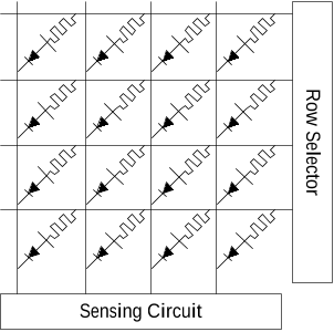
Figure 9: Simple memory array with 1D1M used for each memory cell. ![Table 1: Detailed comparison between memristor-based memory, traditional memories, and other emerging memories according to the 2011 ITRS report [1]. The abbreviations used are: T – transistor, C – capacitor, R – resistor, and D – diode. The bold font indicates the best value per row.](/figures/table-1-detailed-comparison-between-memristor-based-memory-1jvhbfr7.png)
Table 1: Detailed comparison between memristor-based memory, traditional memories, and other emerging memories according to the 2011 ITRS report [1]. The abbreviations used are: T – transistor, C – capacitor, R – resistor, and D – diode. The bold font indicates the best value per row. 
Figure 11: Examples of different organizations with different aspect ratios for a 16-cell memory array. 
Figure 12: Noise margin (∆′) versus aspect ratio for different array sizes. 
Figure 13: Structure of the proposed memristor gated array, where an example of selected of selected cell is shown. 
Figure 4: Traditinal CMOS noise margines, where Voh and Vol are the maximum and the minimum voltage outputs of the circuit respectively. NMH abbreviates Noise Margin High and NML abbreviates Noise Margin Low. 
Figure 3: Two equivalent arrays from the sneak paths point of view. 
Figure 2: The reading current path through a memristor memory array and the equivalent circuit for (a) the ideal case where the current flows only through the target cell and (b) an example of a real case where current sneaks through different undesired paths. The green lines show the desired path and the red ones show the effective sneak paths. 
Figure 14: Noise margins (∆′) versus the array size for the normal array with floating terminals and the new introduced memistor gated array for “All Ones” data set. Also the ratio between the two results are shown in green color on the secondary axis. 
Figure 15: Average power consumption versus the array size for the normal array with floating terminals and the new introduced memistor gated array for “All Ones” data set. 
Figure 5: Noise margins (∆′) versus the array size containing four different data sets. 
Figure 8: Unfolded architecture. 
Figure 6: Power consumption versus array size plotted logarithmically for the cases of grounded and floating array terminals. The dotted line shows the ideal case without the sneak paths effect. 
Figure 7: Ratio of power consumptions and noise margins for the grounded array versus the floating one.


![Table 1: Detailed comparison between memristor-based memory, traditional memories, and other emerging memories according to the 2011 ITRS report [1]. The abbreviations used are: T – transistor, C – capacitor, R – resistor, and D – diode. The bold font indicates the best value per row.](/figures/table-1-detailed-comparison-between-memristor-based-memory-1jvhbfr7.webp)


Citations
526 citations
258 citations
Cites background from "Memristor-based memory"
...This sneak path current [43]–[46] does not change the state of any memristor since the isolation voltage is lower than threshold voltage....
[...]
...Several approaches are proposed to overcome this problem [43], [44], [47]....
[...]
...One of the primary concerns associated with this operation is the sneak path phenomenon [43]–[46], which is an...
[...]
201 citations
Additional excerpts
...There are several designs of memory-based computing and storage architectures with on memristive devices [99], [88] used for various applications, such as computation, image, and video processing [100]....
[...]
163 citations
Cites background from "Memristor-based memory"
...The training process is not affected by sneak path currents [47]....
[...]
159 citations
References
8,971 citations
7,585 citations
Additional excerpts
...Keywords: Nanotechnology, Memory, Memory Array, Memristor, Sneak Paths...
[...]
3,650 citations
1,208 citations
1,097 citations
"Memristor-based memory" refers background in this paper
...Email addresses: mohammed.zidan@kaust.edu.sa (Mohammed Affan Zidan), hfahmy@alumni.stanford.edu (Hossam Aly Hassan Fahmy), muhammadmustafa.hussain@kaust.edu.sa (Muhammad Mustafa Hussain), khaled.salama@kaust.edu.sa (Khaled Nabil Salama) One of the main challenges facing the memristor at the circuit…...
[...]