scispace - formally typeset
Open AccessJournal ArticleDOI

Microfabrication of gold wires for atom guides

Reads0
Chats0
TLDR
In this paper, the feasibility and the suitability of the fabrication process based on gold sputtering technique to realize such devices were discussed and a lower cost technique based on Gold electroplating was considered.
Abstract
Miniaturised atom optics is a new field allowing the control of cold atoms in microscopic magnetic traps and waveguides. Using microstructures (hereafter referred to as atom chips), the control of cold atoms on the micrometer scale becomes possible. Applications range from integrated atom interferometers to the realisation of quantum gates. The implementation of such structures requires high magnetic field gradients. The motivation of this work was to develop a suitable fabrication process for micromachined high-density current-carrying wires for atom guides. However, the developed process may be used for a variety of applications such as on-chip inductors and microtransformers. In order to realise the micromachined wires for atom guides different designs and fabrication processes were investigated. We discuss the feasibility and the suitability of the fabrication process based on gold sputtering technique to realise such devices. As an alternative we have considered a lower cost technique based on gold electroplating. For the electroplating we used commercial full bright cyanide free gold plating solution (gold sulphite, mild alkaline solution with pH = 9 Gold ECF 60, brightener E3) containing 10 g/dm3 gold from Metalor. Some analytical and measurement results of magnetic atom traps are also presented in this paper.

read more

Content maybe subject to copyright    Report

Sensors and Actuators A 115 (2004) 600–607
Microfabrication of gold wires for atom guides
E. Koukharenko
a,
, Z. Moktadir
a
, M. Kraft
a
, M.E. Abdelsalam
c
,
D.M. Bagnall
a
,C.Vale
b
, M.P.A. Jones
b
, E.A. Hinds
b
a
School of Electronics and Computer Science, University of Southampton, Highfield, Southampton SO17 1BJ, UK
b
Blackett Laboratory, Imperial College, Prince Consort Road, London SW7 2BW, UK
c
School of Chemistry Department, University of Southampton, Southampton, UK
Received 22 September 2003; received in revised form 27 February 2004; accepted 4 March 2004
Available online 7 June 2004
Abstract
Miniaturised atom optics is a new field allowing the control of cold atoms in microscopic magnetic traps and waveguides. Using
microstructures (hereafter referred to as atom chips), the control of cold atoms on the micrometer scale becomes possible. Applications
range from integrated atom interferometers to the realisation of quantum gates. The implementation of such structures requires high
magnetic field gradients.
The motivation of this work was to develop a suitable fabrication process for micromachined high-density current-carrying wires for
atom guides. However, the developed process may be used for a variety of applications such as on-chip inductors and microtransformers.
In order to realise the micromachined wires for atom guides different designs and fabrication processes were investigated. We discuss the
feasibility and the suitability of the fabrication process based on gold sputtering technique to realise such devices. As an alternative we have
considered a lower cost technique based on gold electroplating. For the electroplating we used commercial full bright cyanide free gold
plating solution (gold sulphite, mild alkaline solution with pH = 9 Gold ECF 60, brightener E3) containing 10g/dm
3
gold from Metalor.
Some analytical and measurement results of magnetic atom traps are also presented in this paper.
© 2004 Elsevier B.V. All rights reserved.
Keywords: Atom guide; Gold wires; High density currents; Sputtering; Electroplating; SPR 220-7; Thick photoresist
1. Introduction
In the last few years considerable interest in the design of
microscopic atom traps for manipulating neutral atoms has
developed. Miniature atom traps have potential applications
in many fields including quantum computing and integrated
atom optics. Microfabricated current-carrying wires can pro-
duce magnetic fields suitable for trapping atoms that are laser
cooled to K temperatures; this is depicted schematically
in Fig. 1. Recently, Bose–Einstein condensed atom clouds
have been produced using micrometer-sized atom traps fab-
ricated on chips [1,2]. This paves the way to a field where
microelectromechanical systems (MEMS) and atom optics
overlap. Microfabrication can bring a significant contribu-
tion to this field due to the advanced techniques used to fab-
ricate micron scale structures. The overlap between the two
Corresponding author. Tel.: +44-23-80-593-127;
fax: +44-23-80-593-029.
E-mail address: ak@ecs.soton.ac.uk (E. Koukharenko).
fields is expected to lead to a range of interesting devices
for sensing applications and quantum computing.
The purpose of this work is the microfabrication of wires
capable of carrying high density currents necessary to create
high magnetic field gradients used for atom trapping. The
development of a suitable fabrication process for gold wires
for atom chips is a challenging task. There are mainly three
different techniques that could be considered: gold evapo-
ration, sputtering or electroplating; all having their advan-
tages and disadvantages. The trade-off is cost of fabrication
versus ease of fabrication. In this work we discuss the fea-
sibility of gold sputtering technique and electroplating as an
alternative.
2. Atom trapping
Neutral atoms with an unpaired electron have a mag-
netic dipole moment, and interact with magnetic fields. The
sign of the interaction depends on the orientation of the
dipole with respect to the magnetic field. If the atoms have a
0924-4247/$ see front matter © 2004 Elsevier B.V. All rights reserved.
doi:10.1016/j.sna.2004.03.069

E. Koukharenko et al. /Sensors and Actuators A 115 (2004) 600–607 601
Fig. 1. Schematic representation of an atom cloud in the vicinity of high current density carrying wires.
lower energy in regions of a low magnetic field, they can be
trapped and guided using magnetic field minima. Creating
these magnetic fields using microfabricated wires on a chip
allows the atoms to be trapped and guided close to the sur-
face, and the flexible geometry of the wires allows a wide
variety of trapping potentials to be produced. Fig. 2 shows
contour plots of the magnetic field produced by two wires
showing the minimas of the magnetic field where atoms can
be trapped. These simulations were made for three different
values of the current. For example, the combination with an
external magnetic bias field, two parallel wires carrying a
current of a few Amperes allow the creation of a waveguide
that can be split and recombined simply by varying the bias
field. One target application of this work is an atom inter-
ferometer.
The magnetic dipole interaction is quite weak, and hence
the atoms must be pre-cooled to <100 mK before they can
be trapped. This is achieved using laser cooling techniques.
The gold surface in parts of the fabricated atom chips forms
Fig. 2. Contour plot of the magnetic field produced by two wires showing the minimas of the magnetic field where atoms are trapped. These simulations
were made for three different values of the current.
a good mirror, which is used to reflect some of the light,
used to cool the atoms. Once the chip is loaded, the atoms
can be cooled further using radiofrequency evaporative
cooling. This allows the atoms to be cooled to 300 nK. At
temperatures this low, bosonic atoms such as
87
Rb will
undergo Bose–Einstein condensation. The resulting atom
cloud is a giant “coherent matter wave”. Using a simple
atom chip based on a single macroscopic wire, we have
successfully produced Bose–Einstein condensates of
87
Rb
containing 5 × 10
4
atoms. Fig. 3 shows absorption im-
ages of atom clouds; the sharp peaks are the signature of
Bose–Einstein condensation on a chip. Combining this con-
densate with the wide variety of magnetic potentials that
can be produced by microfabrication techniques will open
up many possibilities for coherent control of matter waves;
one example is atom interferometry.
Cold atoms trapped on atom chips have already been used
as a highly sensitive probe of the magnetic field fluctuations
above a conducting wire [3].

602 E. Koukharenko et al. / Sensors and Actuators A 115 (2004) 600–607
Fig. 3. Absorption images of atom clouds; the sharp peaks are the typical
signature of Bose–Einstein condensation on a chip.
3. Fabrication process techniques
3.1. Sputtering technique
The challenge of the fabrication technique is to produce
thick, high density current-carrying gold wires. From sim-
ulations of the magnetic field a thickness of the gold wires
between 5 and 10m was found to be suitable. Additionally,
the surface of gold wires has to be very smooth since rough-
ness of the surface may cause a non-homogeneous current
distribution.
The first fabrication process that was developed in this
work is based upon sputtering and wet etching of a thick
gold layer. The full fabrication process flow is described in
the following:
(10 0) silicon wafers (p-type, 17–33 cm resistivity,
100mm in diameter) were cleaned in fuming nitric acid
(FNA) for 10 min, followed by rinsing in de-ionised wa-
ter and spin-dryed in a nitrogen environment. Next, a thin
electrical insulating film of silicon dioxide SiO
2
(600nm)
was deposited by wet oxidation. Then, few hundreds of
Angstroms of Cr were sputtered on four different wafers as
an adhesion layer. Next, layers of Au with thickness of 3,
5, 10 and 25 m were deposited on the top.
This was followed by a spin-coating step to deposit
standard photoresist (S1818) using a hand spinner. Then,
the gold layers were photolithographically patterned with
a mask to form the areas for the contacts pads, the gold
wires, and the gold mirrors. The mask design is shown in
Fig. 4. The four central wires, above which atom clouds
can be trapped, were 50 and 100 m wide, 7 mm long and
separated by a gap of 30m. The transverse wires were
45 and 90 m wide and 11 mm long. The exposure was
done with a contact mask using a hybrid technology group
(HTG) aligner using UV lights source (350–450nm spec-
trum, mercury lamp) at 1.6–1.9 mW/cm
2
intensity. The next
step was wet chemical etching of Au with aqueous KI
3
so-
lution (4 g KI, 1g I
2
in 40 ml H
2
O) and then Cr in a mixture
of a ceric ammonium nitrate (H
8
CeN
8
O
18
) with nitric acid
(5g H
8
CeN
8
O
18
, 4 ml HNO
3
(70%) in 5 ml H
2
O) [4]. The
Fig. 4. Mask design used for wire fabrication.
process flow is diagrammatically illustrated in Fig. 5.A
first prototype device was fabricated using this technique.
3.2. Electroplating technique
Despite of the fact that a fabrication technique based on
sputtering was found to be suitable for our applications, it
is a time-consuming and a costly process. Thus, we decided
to develop an alternative fabrication technique. Electroplat-
ing is a promising technique for the fabrication of MEMS
in general. It has a number of significant advantages. First,
electrochemical deposition produces a high density of the
deposited material in the holes of the template (mould) and
leads to volume templating of the structure as opposed to
templating of material. As a result there is no shrinkage of
the material when the template is removed and no need for
further processing steps or the use of elevated temperatures.
In consequence, the resulting metal film is a true cast of the
template structure and the size is directly determined by the
Fig. 5. Fabrication process flow using sputtering technique.

E. Koukharenko et al. / Sensors and Actuators A 115 (2004) 600–607 603
Fig. 6. Fabrication process flow for the gold electroplating test batch.
size of the template used. Secondly, electrodeposition can be
used to prepare a wide range of materials from both aqueous
and non-aqueous solutions under conditions, which are com-
patible with the template. Thirdly, electrochemical deposi-
tion allows fine control over the thickness of the resulting
film by controlling of the total charge passed to deposit the
film. This is a unique feature of the approach. Various mate-
rial properties, such as the grain size and surface roughness,
can be controlled by the electroplating conditions [5,6].
Fourthly, electrochemical deposition is ideal for the pro-
duction of thin supported layers for applications such as
photonic mirrors since the surface of the electrochemically
deposited film can be very uniform [7].
A batch to check the suitability of thick gold electroplated
films for atom guides was developed. An important aspect
is to find a compatible photoresist with the gold sulphite
Fig. 8. SEM picture showing the central region the wires structure.
Fig. 7. Fabrication process flow for the gold electroplating and evaporation
techniques.
alkaline plating solution. The process steps are summarised
as follow: the same silicon wafers as for the first process
were used. After a standard cleaning process a thin layer of
Cr/Au (40, 300 nm) was evaporated. The Au layer served
as a seed layer for electroplating. In order to make the sur-
face as clean as possible a preliminary cleaning was nec-
essary, which was done by immersing the wafer into IPA
solution for 10 min. This was followed by spin-coating of
thick positive photoresist SPR 220-7 (up to 14 m) which
later was used as a mould for the gold electroplating [8,9].
This thickness was achieved with a single layer coating to
get good contact between the mask and the wafer we had
to remove the photoresist edge bead which was formed dur-
ing the low-speed coating. This was achieved by exposing

604 E. Koukharenko et al. / Sensors and Actuators A 115 (2004) 600–607
Fig. 9. SEM side view of gold wires fabricated by sputtering.
the edges of the wafer for 700 s and developing for 2 min.
The resist was photolithographically patterned with the mask
shown in Fig. 4 to define the areas for electroplating. Once
the photoresist moulds were fabricated, electroplating of Au
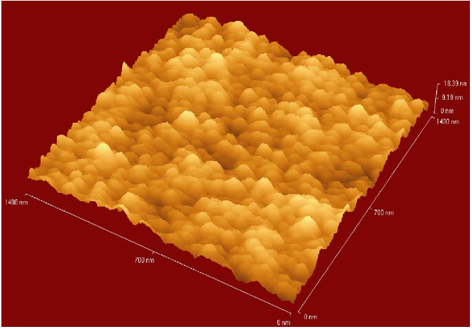
Fig. 10. AFM roughness measurement for gold wires fabricated by sputtering. The r.m.s. roughness is about 16 nm.
was performed without a hardbaking the photoresist since
this can cause SPR 220-7 to reflow.
Electrochemical deposition was performed in a ther-
mostatically controlled cell at 25
C using a conventional

Citations
More filters
DissertationDOI

Production and oscillations of a Bose Einstein condensate on an atom chip

Benjamin Yuen
TL;DR: In this article, a Bose-Einstein condensate of approximately 2 × 10⁴ 87Rb atoms, trapped at the surface of an atom chip, is shown to experience significant damping with an 1/e decay rate which varies between 2 s− 1 and 8 s−1, depending on the fraction of non-condensed atoms in the gas.
Journal ArticleDOI

Digital biomagnetism: Electrodeposited multilayer magnetic barcodes

TL;DR: A magnetic encoding technique for performing high-throughput biological assays is presented in this article, where a gold cap facilitates the growth of self-assembled monolayers (SAMs), while microdrop printing allows efficient generation of large libraries of tagged probes.
Dissertation

Fabrication of an Atom Chip for Rydberg Atom-Metal Surface Interaction Studies

Owen Cherry
TL;DR: In this paper, two atom chips for the study of interactions between 87Rb Rydberg atoms and a Au surface were fabricated using thermally evaporated Cr/Au and patterned using lift-off photolithography.
Book ChapterDOI

Circuit Approach for Simulation of EM-quantum Components

TL;DR: The circuit approach to describe the quantummechanical phenomena is pertinent for seamless simulation of the future-generation integration, although the main attention in this Chapter is paid to the modeling of trapped Bose-Einstein condensates.
References
More filters
Book

Micromachined Transducers Sourcebook

TL;DR: In this paper, the authors present an overview of Micromachining Techniques, Mechanical Transducers, Optical Transducers and Ionizing Radiation Transducers for Microfluidic Devices.
Journal ArticleDOI

Bose–Einstein condensation on a microelectronic chip

TL;DR: It is demonstrated that the formation of a condensate can be greatly simplified using a microscopic magnetic trap on a chip, and the possibility of manipulating laser-like coherent matter waves with such an integrated atom-optical system holds promise for applications in interferometry, holography, microscopy, atom lithography and quantum information processing.
Journal ArticleDOI

Bose-Einstein condensation in a surface microtrap.

TL;DR: Bose-Einstein condensation has been achieved in a magnetic surface microtrap with 4 x 10(5) (87)Rb atoms in a vacuo trap design compatible with ultrahigh vacuum below 2 x 10(-11) mbar.
Journal ArticleDOI

Spin coupling between cold atoms and the thermal fluctuations of a metal surface.

TL;DR: The loss of atoms from the microtrap due to spin flips are observed, induced by radio-frequency thermal fluctuations of the magnetic field near the surface, as predicted but not previously observed.
Journal ArticleDOI

Optical properties of nanostructured metal films

TL;DR: The reflection spectra of the films at normal incidence were recorded as a function of film thickness and the spectra correlated with the local visual appearance of the film and the surface structure from SEM, showing a single reflectivity dip at a wavelength just below the sphere diameter consistent with surface-plasmon grating-like behaviour.
Related Papers (5)
Frequently Asked Questions (14)
Q1. What contributions have the authors mentioned in the paper "Microfabrication of gold wires for atom guides" ?

The motivation of this work was to develop a suitable fabrication process for micromachined high-density current-carrying wires for atom guides. The authors discuss the feasibility and the suitability of the fabrication process based on gold sputtering technique to realise such devices. As an alternative the authors have considered a lower cost technique based on gold electroplating. Some analytical and measurement results of magnetic atom traps are also presented in this paper. 

The r.m.s. surface roughness of gold wires is about 16 nm, which is expected to be low enough to make it suitable for atom trapping applications. 

For their applications a very smooth mirror surface, which is crucial for realising the optics for the laser cooling of the atom clouds [11]. 

The gold substrate with the template was the working electrode with a large area platinum gauze counter electrode and a custom-made saturated calomel reference electrode (SCE). 

the surface of gold wires has to be very smooth since roughness of the surface may cause a non-homogeneous current distribution. 

4. The four central wires, above which atom clouds can be trapped, were 50 and 100 m wide, 7 mm long and separated by a gap of 30 m. 

electrochemical deposition is ideal for the production of thin supported layers for applications such as photonic mirrors since the surface of the electrochemically deposited film can be very uniform [7]. 

a thin Au–Cr layer (40, 300 nm) is evaporated and photolithographically patterned using a standard thin photoresist (SPRT 518) in order to define electroplating areas for gold wires, to provide electrical isolation between gold mirrors, gold wires, and contact pads. 

Using a simple atom chip based on a single macroscopic wire, the authors have successfully produced Bose–Einstein condensates of 87Rb containing 5 × 10⁴ atoms. 

Once the photoresist moulds were fabricated, electroplating of Auwas performed without a hardbaking the photoresist since this can cause SPR 220-7 to reflow. 

This is important for uniform current distribution which is required to obtain a high current density in the wire necessary for an atom guide. 

One problem with the described electroplating is that the achievable smoothness is not sufficient for the gold mirrors without further optimisation of the electroplating solution using special additives such as brighteners. 

This thickness was achieved with a single layer coating to get good contact between the mask and the wafer the authors had to remove the photoresist edge bead which was formed during the low-speed coating. 

electrochemical deposition produces a high density of the deposited material in the holes of the template (mould) and leads to volume templating of the structure as opposed to templating of material.