This document is the unedited Author’s version of a Submitted Work that was subsequently accepted
for publication in ACS Energy Letters, copyright © American Chemical Society after peer review. To
access the final edited and published work see
https://pubs.acs.org/doi/full/10.1021/acsenergylett.7b01279

Accepted: ACS Energy Letters, Jan 2018
1
Stable Dopant-Free Asymmetric Heterocontact Silicon Solar Cells with Efficiencies Above
20%
James Bullock
1,2,‡
, Yimao Wan
1,2,3,‡
, Zhaoran Xu
1,2
, Stephanie Essig
4
, Mark Hettick
1,2
, Hanchen
Wang
1,2
, Wenbo Ji
1,2
, Mathieu Boccard
4
, Andres Cuevas
3
, Christophe Ballif
4
and Ali Javey
1,2,
*
1
Department of Electrical Engineering and Computer Sciences, University of California, Berkeley, California 94720, USA.
2
Materials Sciences Division, Lawrence Berkeley National Laboratory, Berkeley, California 94720, USA.
3
Research School of Engineering, The Australian National University (ANU), Canberra, ACT 0200, Australia
4
École Polytechnique Fédérale de Lausanne (EPFL), Institute of Micro Engineering (IMT), Photovoltaics and Thin Film
Electronic Laboratory (PVLab), Maladière 71b, CH-200 Neuchatel, Switzerland
‡
These authors have contributed equally to this work
* corresponding author: Ali Javey (ajavey@berkeley.edu)

Accepted: ACS Energy Letters, Jan 2018
2
Abstract
Development of new device architectures and process technologies are of tremendous
interest in crystalline silicon (c-Si) photovoltaics to drive enhanced performance and/or
reduced processing cost. In this regard, an emerging concept with a high efficiency potential
is to employ low/high work function metal compounds or organic materials to form
asymmetric electron and hole heterocontacts. This paper demonstrates two important
milestones in advancing this burgeoning concept. Firstly, a high-performance, low-
temperature, electron-selective heterocontact is developed, comprised of a surface
passivating a-Si:H layer, a protective TiO
x
interlayer and a low work function LiF
x
/Al outer
electrode. This is combined with a MoO
x
hole-selective heterocontact to demonstrate a cell
efficiency of 20.7% – the highest value for this cell class to date. Secondly, we show that this
cell passes a standard stability test by maintaining >95% of its original performance after
1000 hours of unencapsulated damp-heat exposure, indicating its potential for longevity.
TOC Figure

Accepted: ACS Energy Letters, Jan 2018
3
In recent times, there has been a significant increase in the use of metal oxides,
1–6
fluorides,
7–9
sulphides,
10
and organic materials
11,12
as carrier selective heterocontacts for
crystalline silicon (c-Si) photovoltaic (PV) devices. This research stream has been motivated by
potential advantages associated with fabrication simplicity and cost reduction. Such materials can
be deposited at low temperature (< 200
o
C) using simple techniques, to form full-area
heterocontacts with optical characteristics tailored for either the sunward- or rear-side of a solar
cell. These heterocontacts can also overcome or reduce losses common to other c-Si cell
architectures—for example, parasitic absorption or heavy impurity doping losses
7,13–15
—
increasing the practical efficiency limit of this structure. Most efforts so far have focused on
substituting one such heterocontact into an otherwise conventional c-Si cell,
16–20
demonstrating, in
many cases, clear performance or fabrication advantages. The ultimate extension of this concept
is to use a set of asymmetric heterocontacts in a single cell structure, sometimes referred to as the
dopant-free asymmetric heterocontact or DASH cell. In our previous study, we presented a record
19.4% efficient DASH solar cell,
7
utilizing MoO
x
and LiF
x
based heterocontacts with thin
amorphous silicon (a-Si:H) interfacial passivation layers. Although promising for a first proof-of-
concept, it is important to demonstrate that higher conversion efficiencies can be achieved, in line
with the suggested higher efficiency potential of this architecture. Further, for a new technology
to be considered in a field such as c-Si PV, it must satisfy additional requirements related to thermal
steps during cell and module fabrication and to device longevity in operation. Therefore, in this
study the DASH cell structure is revisited with a particular emphasis on simultaneously improving
the device efficiency and stability. Modifications to the structure and fabrication allow us to show
for the first time that this technology is compatible with efficiencies greater than 20%. We also

Accepted: ACS Energy Letters, Jan 2018
4
show that un-encapsulated DASH devices can pass an accelerated environmental test designed to
simulate the expected damp-heat stressors presented to a solar cell over its lifetime.
To increase the DASH cell performance, improvements must be made simultaneously to
both the electron and hole heterocontacts. A recent study conducted by co-authors has shown the
thermal stability of the hole heterocontact can be improved via an additional annealing step prior
to the MoO
x
deposition.
21
In this study, we focus on the electron side, aiming to develop a
thermally robust rear heterocontact. The electron-selective heterocontact of our first-generation
DASH cell utilized a low work function (~1 nm) LiF
x
/ Al outer stack to efficiently extract
electrons. When applied to c-Si the low work function induces downward band-bending,
encouraging electrons to the surface. To improve the stability of this contact, here we integrate
thin oxide protective layers to prevent interaction between the thin a-Si:H passivation layer and
the LiF
x
/ Al layers, without causing a significant impediment to electron flow. Four candidate
oxides are trialled in this application: Titanium oxide (TiO
x
), Tantalum oxide (Ta
2
O
x
), Hafnium
oxide (HfO
x
) and Aluminium oxide (Al
2
O
x
). All are deposited via atomic layer deposition (ALD)
at temperatures ≤ 150
o
C (further details can be found in Table 1). These materials are chosen to
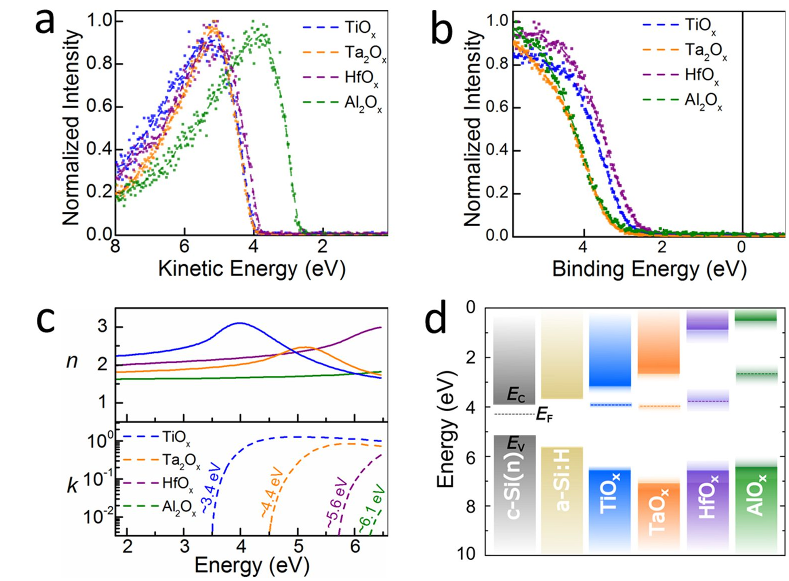
study the influence of conduction band offset on the electron contact performance. To firstly
quantify the conduction band offset, Figure 1 presents the measured optoelectronic properties of
TiO
x
, Ta
2
O
x
, HfO
x
and Al
2
O
x
thin films (~15 nm) deposited on polished c-Si wafers. The work
function and valence band spectrum, measured by X-ray Photoelectron Spectroscopy (XPS), are
presented in Figure 1a and b, respectively. The oxygen and metal core levels are also measured by
XPS, revealing the stoichiometry of TiO
x
(x = 2.02), Ta
2
O
x
(x = 5.0), HfO
x
(x = 1.93) and Al
2
O
x
(x = 2.98). This is accompanied by the refractive indices (n, k) presented in Figure 1c, extracted
from spectroscopic ellipsometry. Implicit within this modelling is a fitting of the optical bandgap


