scispace - formally typeset
Search or ask a question
Journal ArticleDOI

Thermal Modeling and Design Optimization of PCB Vias and Pads

01 Jan 2020-IEEE Transactions on Power Electronics (Institute of Electrical and Electronics Engineers (IEEE))-Vol. 35, Iss: 1, pp 882-900
TL;DR: In this article, an axisymmetric thermal resistance model is developed for PCB thermal pads where the heat conduction, convection, and radiation all exist; due to the interdependence between the conductive/radiative heat transfer coefficients and the board temperatures, an algorithm is proposed to fast obtain the board-ambient thermal resistance and to predict the semiconductor junction temperature.
Abstract: Miniature power semiconductor devices mounted on printed circuit boards (PCBs) are normally cooled by means of PCB vias, copper pads, and/or heatsinks. Various reference PCB thermal designs have been provided by semiconductor manufacturers and researchers. However, the recommendations are not optimal, and there are some discrepancies among them, which may confuse electrical engineers. This paper aims to develop analytical thermal resistance models for PCB vias and pads, and further to obtain the optimal design for thermal resistance minimization. First, the PCB via array is thermally modeled in terms of multiple design parameters. A systematic parametric analysis leads to an optimal trajectory for the via diameter at different PCB specifications. Then, an axisymmetric thermal resistance model is developed for PCB thermal pads where the heat conduction, convection, and radiation all exist; due to the interdependence between the conductive/radiative heat transfer coefficients and the board temperatures, an algorithm is proposed to fast obtain the board-ambient thermal resistance and to predict the semiconductor junction temperature. Finally, the proposed thermal models and design optimization algorithms are verified by computational fluid dynamics simulations and experimental measurements.

Summary (4 min read)

A. Thermal Modeling of PCB Vias

  • A cluster of PCB plated through holes (PTHs), i.e., vias, can provide an effective thermal path, which helps to transfer heat from an SMD (chip) to a heatsink.
  • Also, the attached heatsink has a large heat dissipation capability.
  • Accordingly, the PCB via array in each pattern can be divided into multiple via units, as indicated by the dashed box in Fig. 1 .
  • The general equation for thermal conductivity is [32] / k q T , where q is the heat flux (W/m 2 ) and T represents the temperature gradient (K/m).
  • The standard IPC-6012 specifies a minimum copper plating thickness of 20 µm for Class 1 PCBs, and 25 µm is a standard via plating thickness [37] .

1) Via-to-Via Spacing s

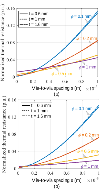
  • Based on (5), the curves of the normalized via thermal resistance with respect to the via-to-via spacing s can be depicted for different filler materials, PCB thicknesses, and via diameters, as shown in Fig. 2 .
  • It is seen that the normalized via thermal resistance via,n always rises when the via-to-via spacing s increases, regardless of the PCB thickness, via filling material and via diameter.
  • Therefore, s should be designed as small as possible in order to reduce the thermal resistance of PCB via array.
  • In practice, however, the allowed minimum via-to-via spacing depends on PCB manufacturing capability and is cost sensitive.
  • Generally, 8 mil (0.2 mm) is a commonly-specified minimum via-to-via spacing by most PCB manufacturers, and therefore, s = 0.2 mm is used in the following analysis and experiments.

2) Number of layers NCu, PCB Thickness t, and Copper Layer Thickness tCu

  • The dependence of the normalized thermal resistance of a PCB via array, via,n, on the number of copper layers NCu, copper thickness tCu, and PCB thickness t is shown in Fig. 3 .
  • As can be seen, the parameters NCu, tCu and t, have a negligible impact on the normalized thermal resistance, implying that the copper and FR4 layers have a much higher thermal resistance compared to the vias.
  • Thus the heat is mainly transferred through the vias, and (5) can be simplified as EQUATION ) ) ).
  • Then, the dependence of the normalized thermal resistance on the via diameter  and the filler material is illustrated in Fig. 4 (b) and (c).
  • When the vias are not filled, the optimal via diameter is about 0.25 mm; if  = 0.8 mm is chosen, then there will be a 44% increase in the thermal resistance.

C. Modeling of Outer-Zone Vias

  • In some cases, the heatsink is larger than the chip, and thus the outer-zone vias can be added around the inner via array to further decrease the equivalent thermal resistance between the case and the heatsink, as shown in Fig. 5 .
  • For the sake of simplicity, only via Pattern I is considered herein.
  • The PCB vias can be divided into two zones, i.e., the inner-zone via array directly beneath the chip, and the outer-zone vias around the inner-zone via array, as illustrated in Fig. 5 (a) and (b).

1) Lumped Thermal Resistance Model

  • Since there is a uniform heat source on the inner via array, and a powerful heatsink beneath the PCB, the radial-direction heat transfer of the inner-zone via array is not pronounced compared with the vertical direction.
  • As for the outer-zone vias, the radial and vertical heat transfers are equally pronounced.
  • Hence, both the distributed radial and vertical thermal resistances are taken into account, as shown in Fig. 5(a) .
  • The cross transformation can be decoupled into a D-Y transformation and a Y-D transformation.
  • Where i represents the copper layer order, and j denotes the outer via layer order.

2) Derivation of Equivalent Thermal Resistance

  • The equivalent thermal resistance of the complicated network shown in Fig. 5(c ) can be derived by performing analog circuit simulations with given radial and vertical thermal resistance values as (8) .
  • There are multiple design variables (e.g., , s, j) and system parameters (l, w, tCu, kfiller, tPTH, NCu, t), which implies that the method of circuit simulation does not support systematical parametric analysis.
  • Therefore, a simple algorithm is developed in MATLAB to obtain the final equivalent thermal resistance of the complicated network (Fig. 5(c) ) with any values.

3) Parametric Analysis

  • Based on the proposed thermal resistance model for outer-zone vias, the dependence of the ultimate thermal resistance of PCB vias on multiple design variables and parameter is plotted in Fig. 8 .
  • If the maximum outer via layer number equals 0, then it means that there are only inner-zone vias.
  • It is seen from Fig. 8 that the thermal resistance decreases with the increase of the outer via layer number.
  • According to Fig. 8 (b), one can conclude that the filler material and via diameter affect the thermal resistance as well.
  • In the case of air filling, the optimal diameter is 0.25 mm.

III. THERMAL MODELING AND SIZING OF PCB PADS

  • For the natural convection in the air, the flow remains laminar when the temperature difference involved is less than 100 o C and the characteristic length of the body is less than 0.5 m [38] , which is almost always the case in electronic systems.
  • When the PCB is composed of FR4 only (i.e., NCutCu = 0), its in-plane thermal conductivity reaches the minimum kFR4.
  • Hence, the rectangular heat source and PCB pad are transformed to axisymmetric circular ones based on ensuring that the total area remains the same, as shown in Fig. 9(b ).
  • As discussed in Section III-A, PCB pads can be regarded thin due to the negligible temperature drop over the vertical direction.
  • Manipulating ( 21) and ( 23) yields the equivalent thermal resistance from rs to the ambient and the thermal resistance from re to the ambient when an axisymmetric heat source is located at rb.

D. Algorithm for Copper Pad Sizing

  • When an SMD is mounted on a PCB, the heat generated inside the device will dissipate in two parallel pathways: one is from the junction, then to the top case, and finally to the ambient; the other is from the junction to the bottom case, then to the board, and finally to the ambient.
  • Hence, the thermal resistances ta and ba are temperature dependent.
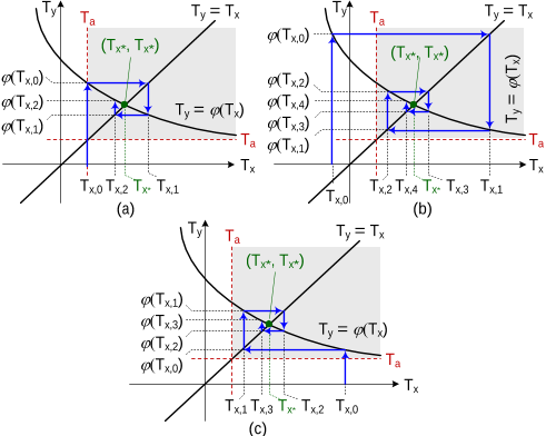
  • Therefore, the initial iteration value of Tx,0 .
  • A fixed-point iteration based algorithm taking into account all the five thermal resistances shown in Fig. 12 is developed to design the copper pad size, as shown in Fig. 14 .
  • If all four temperatures errors are smaller than lmt, then the algorithm proceeds to calculate the junction temperature Tj according to (31) .

Give an initial temperature T e,g

  • The average elapsed times are as short as approximately 30 ms.
  • Personal use is permitted, but republication/redistribution requires IEEE permission.
  • Selected initial iteration values, which agrees well with previous analysis.
  • Nevertheless, the iteration can be further accelerated by using advanced methods, e.g., the Aitken's delta-squared process [47] and the Steffensen's method [48] .  t = T t,c -T t,.

E. Thermal Modeling of DPAK Package

  • Apart from the board to ambient thermal resistance ba, the realization of the proposed algorithm shown in Fig. 14 also requires the knowledge of the other four thermal resistances cb, jt, ta, and jc.
  • Therefore, the detailed structure model and simplified package outline dimensions of DPAK package are derived, as shown in Fig. 16 .
  • An analytical model of the thermal resistance ta is firstly developed.
  • Its side and top surfaces are cooled by natural convection and radiation.
  • Assume that the package is placed horizontally, and its surfaces share the same temperature Tt. For the horizontal top surfaces of the molding resin and die pad (see Fig. 16(b) ), their areas are Based on [38] , the characteristic lengths of the two rectangular surfaces under natural convection can be calculated as , respectively.

B. Experimental Verifications

  • A curve tracer B1506A from Keysight Technologies is used to measure the I-V characteristics of a batch of VS-6EWL06FN-M3 diodes, as shown in Fig. 21 Each diode is soldered on a heatsink-cooled PCB with a specified via design.
  • The maximum operating junction temperature of the selected diode VS-6EWL06FN-M3 is 175 o C [49] .
  • In contrast, the existing model provides a minimum copper radius of 6.1 mm, which corresponds to an around 375% increase for the copper pad area compared to the design of re = 2.8 mm.
  • To make a comparison, the results from the existing model and the proposed model (24) are shown in Fig. 25(c ) as well.
  • Therefore, the proposed thermal models enable engineers to fast and easily optimize the design of PCB vias and thermal pads.

Did you find this useful? Give us your feedback

Figures (25)

Content maybe subject to copyright    Report

0885-8993 (c) 2018 IEEE. Personal use is permitted, but republication/redistribution requires IEEE permission. See http://www.ieee.org/publications_standards/publications/rights/index.html for more information.
This article has been accepted for publication in a future issue of this journal, but has not been fully edited. Content may change prior to final publication. Citation information: DOI 10.1109/TPEL.2019.2915029, IEEE
Transactions on Power Electronics
IEEE TRANSACTIONS ON POWER ELECTRONICS
Yanfeng Shen, Member, IEEE, Huai Wang, Senior Member, IEEE, Frede Blaabjerg, Fellow, IEEE,
Hui Zhao, Member, IEEE, and Teng Long, Member, IEEE
Abstract Miniature power semiconductor devices mounted on
printed circuit boards (PCBs) are normally cooled by means of
PCB vias, copper pads, and/or heatsinks. Various reference PCB
thermal designs have been provided by semiconductor
manufacturers and researchers. However, the recommendations
are not optimal, and there are some discrepancies among them,
which may confuse electrical engineers. This paper aims to develop
analytical thermal resistance models for PCB vias and pads, and
further to obtain the optimal design for thermal resistance
minimization. Firstly, the PCB via array is thermally modeled in
terms of multiple design parameters. A systematic parametric
analysis leads to an optimal trajectory for the via diameter at
different PCB specifications. Then an axisymmetric thermal
resistance model is developed for PCB thermal pads where the
heat conduction, convection and radiation all exist; due to the
interdependence between the conductive/radiative heat transfer
coefficients and the board temperatures, an algorithm is proposed
to fast obtain the board-ambient thermal resistance and to predict
the semiconductor junction temperature. Finally, the proposed
thermal models and design optimization algorithms are verified by
computational fluid dynamics (CFD) simulations and
experimental measurements.
Index terms thermal resistance model, thermal management,
printed circuit board (PCB), PCB via, thermal pad.
NOMENCLATURE
Bi Biot number
h Heat transfer coefficient (W/(m
2
·K))
h
conv
Convective heat transfer coefficient (W/(m
2
·K))
h
radi
Radiative heat transfer coefficient (W/(m
2
·K))
k Thermal conductivity of a material (W/(m·K))
k
1
Lateral thermal conductivity of the copper zone
(W/(m
2
·K))
k
2
Lateral thermal conductivity of the FR4 zone
(W/(m
2
·K))
k
Cu
Thermal conductivity of copper (W/(m
2
·K))
k
FR4
Thermal conductivity of FR4 (W/(m
2
·K))
k
filler
Thermal conductivity of via filling material (W/(m
2
·K))
l Length of a via array (m)
L
c
Characteristic length of a hot plate (m)
m
1
Number of rows of a via array in Pattern I
m
2
Number of rows of a via array in Pattern II
n
1
Number of columns of a via array in Pattern I
n
2
Number of columns of a via array in Pattern II
N
Cu
Number of copper layers in a PCB
P Power loss generated by a heat source (W)
q Heat flux (W/m
2
)
r
b
Radius of heat source (package) (m)
r
s
Radius of middle (copper) zone (m)
r
e
Radius of outer (FR4) zone (m)
s Via-to-via spacing (m)
t PCB thickness(m)
t
Cu
Thickness of a PCB copper layer (m)
t
PTH
Plating thickness of PCB vias (m)
T
b
PCB board (r = r
b
) temperature (
o
C)
T
c
Case temperature of a package (chip) (
o
C)
T
j
Junction temperature of a chip (
o
C)
T
t
Top case temperature of a package (chip) (
o
C)
T
a
Ambient temperature (
o
C)
w Width of a via array (m)
Emissivity of PCB surface
ba
Thermal resistance from the inner zone edge (r = r
b
) to
the ambient (
o
C/W)
barrel
Vertical thermal resistance of the copper barrel in a via
unit (
o
C/W)
cb
Thermal resistance from the case to the PCB (r = r
b
)
(
o
C/W)
unit
Vertical thermal resistance of a via unit (
o
C/W)
Cu
Vertical thermal resistance of the copper layers in a via
unit (
o
C/W)
filler
Vertical thermal resistance of the filler in a via unit
(
o
C/W)
FR4
Vertical thermal resistance of the FR4 layers in a via
unit (
o
C/W)
jc
Thermal resistance from the junction to the case (
o
C/W)
jt
Thermal resistance from the junction to the top case
(
o
C/W)
r,ij
Radial thermal resistance between outer-zone via layers
(
o
C/W)
sa
Thermal resistance from the copper zone edge (r = r
s
)
to the ambient (
o
C/W)
Thermal Modeling and Design Optimization of
PCB Vias and Pads
Part of this work was presented at the 10
th
IEEE Energy Conversion
Congress & Expo (ECCE2018), Portland, USA, and the 29
th
European
Symposium on Reliability of Electron Devices, Failure Physics and
Analysis (ESREF2018), Aalborg, Denmark. This work was supported
by the Innovation Fund Denmark through the Advanced Power
Electronic Technology and Tools (APETT) project. (Corresponding
authors: Teng Long and Yanfeng Shen).
Y. Shen, H. Zhao and T. Long are with the Department of
EngineeringElectrical Engineering Division, University of
Cambridge, Cambridge CB3 0FA, United Kingdom (e-mail:
ys523@cam.ac.uk, hz352@cam.ac.uk, tl322@cam.ac.uk)
H. Wang, and F. Blaabjerg are with the Center of Reliable Power
Electronics (CORPE), Department of Energy Technology, Aalborg
University, Aalborg 9220, Denmark (e-mail: hwa@et.aau.dk,
fbl@et.aau.dk).

0885-8993 (c) 2018 IEEE. Personal use is permitted, but republication/redistribution requires IEEE permission. See http://www.ieee.org/publications_standards/publications/rights/index.html for more information.
This article has been accepted for publication in a future issue of this journal, but has not been fully edited. Content may change prior to final publication. Citation information: DOI 10.1109/TPEL.2019.2915029, IEEE
Transactions on Power Electronics
ta
Thermal resistance from the top case of the chip to the
ambient (
o
C/W)
via
Vertical thermal resistance of a via array (
o
C/W)
via,n
Normalized vertical thermal resistance of a via array
v,ij
Vertical thermal resistance between copper layers of
outer-zone vias (
o
C/W)
Convective heat transfer parameter depending on PCB
geometry and orientation
Stefan-Boltzmann constant
= 5.670367×10
8
(Wm
2
K
4
)
Time (s)
Via diameter (m)
opt
Optimal via diameter (m)
ea
Equivalent thermal resistance from the FR4 zone edge
(r = r
e
) to the ambient (
o
C/W)
sa
Equivalent thermal resistance from the copper zone
edge (r = r
s
) to the ambient (
o
C/W)
ta
Equivalent thermal resistance from the top case of a
package to the ambient (
o
C/W)
I. INTRODUCTION
The volume of modern power semiconductor devices (e.g.,
GaN transistors) are continuingly shrinking in order to achieve
higher power densities, lower parasitic inductances, and lower
power losses [1]-[3]. However, thermal management has been
identified as the main barrier for further power density increase
[4]. The heat generated inside the miniaturized semiconductors
must be effectively dissipated to the ambient; otherwise, the
high junction and board temperatures may cause serious
reliability issues to the semiconductor, solder, thermal grease,
and printed circuit board (PCB) [5]-[8]. In addition, suitable
heat dissipation measures should be considered as early as in
the design and development phase, because subsequent
modifications are generally more costly and involve increased
engineering effort [9], [10].
In medium power applications, the surface-mounted devices
(SMDs) are normally cooled by a heatsink attached to the PCB,
where the thermal via array provides an effective thermal path
for the heat transfer [11]-[13]. In low power scenarios, a PCB
copper pad is typically used for heat spreading, and the SMD
can be cooled by natural convection [14]. Many reference
thermal designs can be found from device manufacturers’
websites [14]-[18]. However, several problems remain:
1) the thermal design guidelines recommended by
manufacturers are not optimal, and they are applicable for
specific packages only [15], [16];
2) inconsistent guidelines; for instance, the thermal via
diameter should be designed as large to reduce the thermal
resistance according to [16]; however, [15], [17] and [18]
recommend smaller via diameters and adopt different via
pitches.
Although the computational fluid dynamics (CFD)
simulations feature high accuracy, the model generation time
and computational cost could be fairly high [14]. Moreover,
CFD simulators are expensive and they are not always available
for electrical engineers. Therefore, it is necessary to develop
analytical models which enable fast and accurate design
optimization for thermal vias and pads.
In the literature, many efforts have been devoted to the
optimization of PCB thermal vias. The research in [19]-[21] is
based on either experimental results or CFD simulations; thus,
not all design scenarios are explored, but only some general
design guidelines are provided for specific applications.
Analytical thermal models of vias are built in [11], [22]-[25];
unfortunately, only partial parameters are analyzed, and no
optimal via design is derived.
For the PCB heat transfer characteristics, the heat conduction,
convection and radiation all exist, which makes the thermal
analysis complicated. Texas Instruments have developed an
online PCB thermal calculation tool based on CFD thermal
resistance data of different package sizes and pad dimensions
[26]. However, some important factors (e.g., the PCB thickness,
number of copper layers, and copper thickness) are not taken
into account, and also the online tool does not support design
optimization. In addition to the CFD simulations, some other
numerical calculation methods are developed [27], [28]. The
study in [28] deals with a substrate for a ball grid array package,
where a belt of densely populated vias and two continuous
copper layers are placed; however, the model is complicated
and no CFD or experimental verifications are provided. For
electrical engineers, it is more desirable to have an analytical
thermal model such that the temperatures of devices with
different designs and cooling methods can be fast predicted [29],
[30]. In [14] and [31], an analytical thermal resistance model is
developed for PCB thermal pads; however, the heat transfer
boundary and the convective heat transfer coefficient variation
over the temperature difference are not included, causing
potential errors between calculations and measurements.
This paper proposed two new analytical thermal models for
PCB vias and thermal pads, respectively. For the thermal model
of PCB vias, a systematic parametric analysis is firstly
conducted, which leads to a simplified thermal resistance model.
An optimal design trajectory is then obtained for PCB vias with
different specifications. After that, an analytical axisymmetric
thermal resistance model is proposed for PCB thermal pads.
Taking into account the interdependence between the
convection/radiative heat transfer coefficients and board
temperatures, a simple algorithm is developed to size thermal
pads at different PCB parameters, power losses, ambient
temperatures, and allowed maximum junction temperatures.
Finally, CFD simulations and experimental measurements
verify the developed analytical thermal models. The proposed
models enable electrical engineers to optimize their PCB via
design and thermal pad sizing at lower cost and less time effort.
II. THERMAL MODELING AND DESIGN OPTIMIZATION OF PCB
VIAS
A. Thermal Modeling of PCB Vias
A cluster of PCB plated through holes (PTHs), i.e., vias, can
provide an effective thermal path, which helps to transfer heat
from an SMD (chip) to a heatsink. The vertical structure of a
multilayer PCB with vias is shown in Fig. 1(a). The via
diameter, via-to-via spacing, and via plating thickness are
denoted as
, s, and t
PTH
, respectively. The number of copper
layers and the copper layer thickness are represented by N
Cu
and
t
Cu
, respectively.

0885-8993 (c) 2018 IEEE. Personal use is permitted, but republication/redistribution requires IEEE permission. See http://www.ieee.org/publications_standards/publications/rights/index.html for more information.
This article has been accepted for publication in a future issue of this journal, but has not been fully edited. Content may change prior to final publication. Citation information: DOI 10.1109/TPEL.2019.2915029, IEEE
Transactions on Power Electronics
For the layout of vias, there are various uniform and non-
uniform design options. For the sake of simplicity, this paper
focuses on two simple uniform patterns, denoted as Pattern I
and Pattern II, as illustrated in Fig. 1(b) and (c), respectively.
However, the derived method can be applied to other vias
layout with minor modifications. The length, width, and
thickness of the PCB via array are denoted as l, w, and t,
respectively. Normally, the PCB thickness is much smaller than
its length and width. Also, the attached heatsink has a large heat
dissipation capability. Therefore, it is assumed that the heat
generated inside the SMD is transferred in the vertical direction
only. Accordingly, the PCB via array in each pattern can be
divided into multiple via units, as indicated by the dashed box
in Fig. 1. It is seen from the horizontal cross-sections of the via
array that the basic via unit in Pattern I is a square of (
+ s) ×
(
+ s), whereas that in Pattern II is rectangular with [
3(
+
s)/2] × (
+ s). If the PCB via array size (l and w) and via
parameters (
and s) are fixed, and the array parameters (l and
w) are much larger than the via unit parameters (
and s), then
the numbers of vias that Patterns I and II can accommodate are
calculated as
11
22
2
2
floor[ / ( )] floor[ / ( )]
/ [( ], Pattern I
floor[ / ( )] floor{2 / [ 3( ]}
2 / [ 3( ], Pattern I
)
)
) I
m n l w
lw
m n l w
l
ss
s
s
w
s
s
(1)
It is seen from (1) that Pattern II can accommodate
approximately
2 / 3 1
= 15.5% more vias than Pattern I.
As can be seen from Fig. 1, there are three vertical thermal
paths for each via unit, i.e., the via filler, the via barrel, and the
copper and flame retardant 4 (FR4) layers, whose vertical
thermal resistances are represented by
barrel
,
filler
, and
Cu
+
FR4
, respectively, as below
2
4
22
2
4
2
,
( / 2
,
(
1
,
)
)
)
)
Pattern I
( / 4
1
, Pattern II
3/2(4/
filler
filler
barrel
Cu
Cu Cu Cu Cu
C
PTH
PTH PTH
Cu FR
u FR
t
kt
t
k t t
N t t N t
kk
s
s
(2)
t
Cu
t
FR4
t
s
(a)
FR4
Copper layer
Filler
Chip
Solder
PCB
TIM
Heatsink
t
PTH
s
t
PTH
s
...
...
...
...
...
...
...
...
× n
1
× m
1
+ s
+ s
l
w
(b)
...
...
...
...
+ s
+ s
s
s
s
+ s
3( ) / 2s
...
...
...
×n
2
×m
2
l
w
(c)
+ s
Via unit
Via unit
Via unit
+ s
filler
FR4
+
Cu
barrel
Fig. 1. Structure and layout of PCB via array. (a) Vertical structure of a
multilayer PCB with vias. Top view of via array in (b) Pattern I and (c) Pattern
II.
where k
filler
, k
Cu
and k
FR4
represent the thermal conductivities of
via filling material, copper, and FR4, respectively. Thus, the
vertical thermal resistance of a via unit can be calculated as
(3)

0885-8993 (c) 2018 IEEE. Personal use is permitted, but republication/redistribution requires IEEE permission. See http://www.ieee.org/publications_standards/publications/rights/index.html for more information.
This article has been accepted for publication in a future issue of this journal, but has not been fully edited. Content may change prior to final publication. Citation information: DOI 10.1109/TPEL.2019.2915029, IEEE
Transactions on Power Electronics
From the perspective of vertical heat transfer, the via units are equivalently connected in parallel, and therefore the total
vertical thermal resistances of a via array of l w t can be obtained as
,
11
,
22
, Pattern I
, Pattern II
unit I
via
unit II
mn
mn
(4)
To simplify the following theoretical analysis, the thermal resistance of a via array is normalized based on the thermal
resistance of an FR4 pad with the same size (l w t), yielding (5).
4
2
4
22
2
4
,
4
]
))
/ ) /
4( )
[4 8 (4 )
( 2 4 (
(
PTH PTH PTH
Cu Cu Cu
c
FR
filler Cu
Cu Cu FR
barr
opper and FR layer
el
fi
s
ller
via
via n
FR
sk
t s s
k t k t t
N t t N t k
t
k lw
k
2
4
22
2
4
4
, Pattern I
2 3( )
[2 3( ) ]
))
//
( 2 4 (
( )
FR
filler Cu
Cu Cu FR
barre
PTH PTH PTH
Cu Cu Cu
copper and F
l
fill
Rl
er
ayers
sk
ts
k t k t t
N t t N t kk
, Pattern II
(5)
B. Parametric Analysis and Design Optimization of PCB
Vias
TABLE I
THERMAL CONDUCTIVITIES OF MATERIALS AT 25
O
C [33]-[36]
Material
Copper
SnAgCu
solder
FR4
Air at
atmospheric
pressure
Through-
plan
In-plane
Thermal
conductivity
393
W/(mK)
57.3
W/(mK)
0.29
W/(mK)
0.81
W/(mK)
0.026
W/(mK)
Since multiple design variables are included in the thermal
resistance model, it is difficult to directly apply (5) in
practical design optimization. Hence, it is necessary to
conduct a parametric analysis on (5).
The thermal conductivity of a material is a measure of its
ability to conduct heat. It is evaluated primarily in terms of
the Fourier’s law for heat conduction. The general equation
for thermal conductivity is [32]
/k q T
, where q is
the heat flux (W/m
2
) and
T
represents the temperature
gradient (K/m). The thermal conductivities of the materials
used in this paper are listed in Table I. The standard IPC-
6012 specifies a minimum copper plating thickness of 20 µm
for Class 1 PCBs, and 25 µm is a standard via plating
thickness [37]. Thus, t
PTH
= 25 µm is used in the following
analysis.
1) Via-to-Via Spacing s
Based on (5), the curves of the normalized via thermal
resistance with respect to the via-to-via spacing s can be
depicted for different filler materials, PCB thicknesses, and
via diameters, as shown in Fig. 2. It is seen that the
normalized via thermal resistance
via,n
always rises when
the via-to-via spacing s increases, regardless of the PCB
thickness, via filling material and via diameter. Therefore, s
should be designed as small as possible in order to reduce the
thermal resistance of PCB via array. In practice, however,
the allowed minimum via-to-via spacing depends on PCB
manufacturing capability and is cost sensitive. Generally, 8
mil (0.2 mm) is a commonly-specified minimum via-to-via
spacing by most PCB manufacturers, and therefore, s = 0.2
mm is used in the following analysis and experiments.
t = 0.6 mm
t = 1 mm
t = 1.6 mm
= 1 mm
= 0.1 mm
= 0.5 mm
= 0.2 mm
(a)
t = 0.6 mm
t = 1 mm
t = 1.6 mm
= 1 mm
= 0.1 mm
= 0.5 mm
= 0.2 mm
(b)
Via-to-via spacing s (m)
Fig. 2. Dependence of the normalized thermal resistance of via array in
Pattern I on the via-to-via spacing s with two via filling materials: (a) air
with a thermal conductivity of 0.026 W/(mK), and (b) solder with a thermal
conductivity of 57.3 W/(mK).

0885-8993 (c) 2018 IEEE. Personal use is permitted, but republication/redistribution requires IEEE permission. See http://www.ieee.org/publications_standards/publications/rights/index.html for more information.
This article has been accepted for publication in a future issue of this journal, but has not been fully edited. Content may change prior to final publication. Citation information: DOI 10.1109/TPEL.2019.2915029, IEEE
Transactions on Power Electronics
= 1 mm
= 0.1 mm
= 0.5 mm
= 0.2 mm
= 1 mm
= 0.1 mm
= 0.5 mm
= 0.2 mm
= 1 mm
= 0.1 mm
= 0.5 mm
= 0.2 mm
= 1 mm
= 0.1 mm
= 0.5 mm
= 0.2 mm
= 1 mm
= 0.1 mm
= 0.5 mm
= 0.2 mm
= 1 mm
= 0.1 mm
= 0.5 mm
= 0.2 mm
0.5 oz, t
l
= 17.5 mm
1 oz, t
l
= 35 mm
0.5 oz, t
l
= 17.5 mm
1 oz, t
l
= 35 mm
0.5 oz, t
l
= 17.5 mm
1 oz, t
l
= 35 mm
2 oz, t
l
= 70 mm
0.5 oz, t
l
= 17.5 mm
1 oz, t
l
= 35 mm
2 oz, t
l
= 70 mm
0.5 oz, t
l
= 17.5 mm
1 oz, t
l
= 35 mm
2 oz, t
l
= 70 mm
0.5 oz, t
l
= 17.5 mm
1 oz, t
l
= 35 mm
2 oz, t
l
= 70 mm
t t t
tt
t
(a) (b) (c)
(d) (e) (f)
N
Cu
N
Cu
N
Cu
N
Cu
N
Cu
N
Cu
t
Cu
t
Cu
t
Cu
t
Cu
t
Cu
t
Cu
t
Cu
t
Cu
t
Cu
t
Cu
t
Cu
t
Cu
t
Cu
t
Cu
t
Cu
t
Cu
0.026
6
0.026
0.026
Fig. 3. Dependence of the normalized thermal resistance of via array in Pattern I on the number of copper layers N
Cu
, copper thickness t
Cu
, and PCB thickness
t with different via filling materials. (a) Air with thermal conductivity k
filler
= 0.026 W(mK) and PCB thickness t = 0.6 mm; (b) Air with thermal conductivity
k
filler
= 0.026 W(mK), PCB thickness t = 1.0 mm; (c) Air with thermal conductivity k
filler
= 0.026 W(mK), PCB thickness t = 1.6 mm; (d) Solder with thermal
conductivity k
filler
= 57.3 W(mK), PCB thickness t = 0.6 mm; (e) Solder with thermal conductivity k
filler
= 57.3 W(mK), PCB thickness t = 1.0 mm; (f) Solder
with thermal conductivity k
filler
= 57.3 W(mK), PCB thickness t = 1.6 mm.
×10
-3
×10
-3
t = 1.6 mm
t = 0.4 mm
k
filler
=0.026W/(mK)
k
filler
=0.35W/(mK)
k
filler
=20W/(mK)
k
filler
= 57.3 W/(mK)
t = 1.6 mm
t = 0.4 mm
Minima
trajectory
s
k
filler
=0.026W/(mK)
k
filler
=0.35W/(mK)
k
filler
=20W/(mK)
k
filler
= 57.3 W/(mK)
Minima
trajectory
(a) (b) (c)
Via diameter Via diameter
s
Fig. 4. (a) Optimal trajectories of via diameter
and via-to-via spacing s with respect to the filler thermal conductivity. Dependence of the normalized
thermal resistance of via array on the diameter
at different PCB thicknesses and filler thermal conductivities for (b) Pattern I and (c) Pattern II.
2) Number of layers N
Cu
, PCB Thickness t, and Copper
Layer Thickness t
Cu
The dependence of the normalized thermal resistance of a
PCB via array,
via,n
, on the number of copper layers N
Cu
,
copper thickness t
Cu
, and PCB thickness t is shown in Fig. 3.
As can be seen, the parameters N
Cu
, t
Cu
and t, have a
negligible impact on the normalized thermal resistance,
implying that the copper and FR4 layers have a much higher
thermal resistance compared to the vias. Thus the heat is
mainly transferred through the vias, and (5) can be simplified
as
2
4
2
,
2
4
2
4( )
,
4 ( ( 2
2 3( )
,
4 ( () 2
))
)
FR
Cu filler
via n
F
PTH PTH PTH
PTH PTH
R
Cu fille PTHr
sk
k t t k t
Pattern I
sk
k t t k t
Pattern II
(6)

Citations
More filters
Journal ArticleDOI
TL;DR: A highly modular, integrated, and compact drive is achieved compared to the nonintegrated version, and an experimental setup is built to validate the results of the introduced multiphysics models.
Abstract: In this article, a circumscribing polygon integrated modular motor drive topology with shared cooling for the power converter and the electrical machine is proposed and benchmarked with the nonintegrated version. The proposed topology is applied on an axial flux permanent magnet synchronous machine. The topology is capable of mechanically mounting the power converter, sufficiently cooling both the power converter and the electrical machine, and combining both of them into the same housing. The mechanical and the thermal design are done to ensure thermal decoupling between the power converter and the motor winding, and to provide a low thermal resistance from the power converter and the electrical machine to the ambient. Due to the limited space available for the power converter module, wide bandgap semiconductor technology is chosen for the implementation of the converter module, thanks to their small package size and low power losses. A highly modular, integrated, and compact drive is achieved compared to the nonintegrated one. A computational fluid dynamics (CFD) model is developed for one module of the proposed integrated drive to evaluate the maximum current that can be injected by one converter module without exceeding the junction temperature limit of the switches and the maximum winding temperature. An experimental setup is built to validate the results of the introduced multiphysics models.

29 citations

Journal ArticleDOI
TL;DR: In this article, coupled electromagnetic-thermal simulations of inductive power transfer (IPT) pads using finite-element simulations are discussed and each electrical and thermal parameters required for the modeling process is outlined.
Abstract: In this article, coupled electromagnetic-thermal simulations of inductive power transfer (IPT) pads using finite-element simulations are discussed Derivation of each electrical and thermal parameters required for the modeling process is outlined Simulation models are used to predict the power loss and the temperature rise of an IPT pad at different ambient temperatures at steady state Using these simulation methods, the power loss within an IPT pad operating at 50 ${^\circ }$ C ambient temperature is predicted A 10-KW IPT system is set up within an environmental chamber to validate the predicted losses within the system

14 citations

Journal ArticleDOI
TL;DR: The electro-thermal design of a discrete half-bridge inverter module for a radially stator mounted axial flux integrated drive is introduced in this paper and the lumped parameter modelling is validated with CFD simulations and experimental measurements.
Abstract: Integrated modular motor drives (IMMDs) have a compact and high fault-tolerant structure compared to their conventional counterparts The most challenging issue in the implementation of these drives is the thermal management of the inverter modules due to the small space available for each module and its physical proximity to the machine windings with their high heat production The electrothermal design of a discrete half-bridge inverter module for a radially stator-mounted (RSM) axial flux integrated drive is introduced in this article The inverter modules are mounted on the stator, radially along the circumference The converter is implemented using GaN technology, and the size is optimized The structure of the presented integration topology from the case of the switches to the cooling ambient is optimized from the thermal point of view The converter is modeled using steady-state and transient lumped parameter thermal networks to estimate the steady state and the instantaneous temperature of the switches The converter parasitics are extracted using FEM simulations, and their influence on the switch loss and temperature is evaluated The lumped parameter modeling is validated with computational fluid dynamics (CFD) simulations and experimental measurements

12 citations


Cites background from "Thermal Modeling and Design Optimiz..."

  • ...The copper layers serve as a heat spreader for better heat transfer [23] and they are also used in effective magnetic field cancellation routing to reduce the parasitics of the converter....

    [...]

Journal ArticleDOI
Yabin Zhang1
TL;DR: In this paper, the Fourier-series analytical solution of temperature and the finite volume method were linked together for thermally modeling the PCB, and thermal-resistance parameters of the components were then used for correlating components' temperatures with the variable arrays in the coupling equations.
Abstract: The previous work relating to the numerical-analytical coupling method for steady-state thermal analysis of the laminated PCB structure is first briefly reviewed. The Fourier-series analytical solution of temperature and the finite volume method were linked together for thermally modeling the PCB. For further modeling the PCB with components, thermal-resistance parameters of the components are then used for correlating components’ temperatures with the variable arrays in the coupling equations. For further considering radiation heat transfer between the PCB and the ambient, an iterative method is proposed. The radiation-equivalent heat transfer coefficient for each surface cell and each component can be updated during the iteration. Moreover, for improving the efficiency, the multigrid strategy is integrated in the coupling method for generating discrete cells of three levels in the metal layer and PCB surface region. To testify the iterative method, the model of a simple one-layer structure is compared with that built in COMSOL Multiphysics. The modeling results of the PCB of a phantom DC-DC power supply under radiation heat transfer are also given and discussed, and the modeling accuracy is approximately derived based on Richardson’s extrapolation.

12 citations

Proceedings ArticleDOI
Jack Knoll1, Gibong Son1, Christina DiMarino1, Qiang Li1, Hannes Stahr, Mike Morianz 
10 Oct 2021
TL;DR: In this paper, the authors presented a PCB-embedded silicon carbide (SiC) MOSFET half-bridge module with low loop inductances, double-sided cooling, and integrated gate driver.
Abstract: This work presents a PCB-embedded silicon carbide (SiC) MOSFET half-bridge module with low loop inductances, double-sided cooling, and integrated gate driver. 1.2 kV SiC MOSFET die are embedded in FR4 using a process developed by AT&S and are electrically connected and cooled through carefully placed copper-filled microvias. The electro-thermal codesign described here limited the power-loop inductance to 2.3 nH and the maximum junction temperature to less than $175 ^{\circ}\mathrm{C}$. Furthermore, integration of the gate drive circuitry within the module limited the gate-loop inductances to 2.2 nH and allowed for a high power density. The measured junction-to-case thermal resistance with double-sided cooling is 0.12 K/W, which is 57 % lower than that of a TO-247 package. A peak efficiency of 98.2 % was achieved when the PCB-embedded half-bridge modules were tested in a 22 kW three-phase ac-dc converter.

9 citations

References
More filters
Book
01 Jan 2011
TL;DR: This book discusses Heat Conduction Equation, Thermal Radiation, and Fundamentals of Convection, as well as other topics related to heating and cooling.
Abstract: TABLE OF CONTENTS Chapter 1- Introduction and Basic Concepts Chapter 2- Heat Conduction Equation Chapter 3- Steady Heat Conduction Chapter 4- Transient Heat Conduction Chapter 5- Numerical Methods in Heat Conduction Chapter 6- Fundamentals of Convection Chapter 7- External Forced Convection Chapter 8- Internal Forced Convection Chapter 9- Natural Convection Chapter 10- Boiling and Condensation Chapter 11- Heat Exchangers Chapter 12- Fundamentals of Thermal Radiation Chapter 13- Radiation Heat Transfer Chapter 14- Mass Transfer Chapter 15 (Web Chapter)- Cooling of Electronic Equipment Chapter 16 (Web Chapter)- Heating and Cooling of Buildings Chapter 17 (Web Chapter)- Refrigeration and Freezing of Foods Appendix 1- Property Tables and Charts (SI Units) Appendix 2- Property Tables and Charts (English Units)

951 citations


"Thermal Modeling and Design Optimiz..." refers background or methods in this paper

  • ...32 is a constant for horizontal plates [38]....

    [...]

  • ...59 is a constant for vertical plates [38]....

    [...]

  • ...The natural convection heat transfer coefficient for laminar flow of air at atmospheric pressure, hconv, and the radiation heat transfer coefficient hradi are [38] ⎧ ⎪⎪⎪⎨ ⎪⎪⎪⎩ hconv = λ[(Tx − Ta)/Lc] hradi = εσ[(Tx + 273) 2 + (Ta + 273) (2)] ×[(Tx + 273) + (Ta + 273)]...

    [...]

  • ...5 m [38], which is almost always the case in electronic systems....

    [...]

  • ...Then, we can obtain the convective heat transfer coefficients of the two top surfaces [38], i....

    [...]

Journal ArticleDOI
TL;DR: In this article, the characteristics and commercial status of both vertical and lateral GaN power devices are reviewed, providing the background necessary to understand the significance of these recent developments and the challenges encountered in GaN-based converter design, such as the consequences of faster switching on gate driver and board layout.
Abstract: Gallium nitride (GaN) power devices are an emerging technology that have only recently become available commercially. This new technology enables the design of converters at higher frequencies and efficiencies than those achievable with conventional Si devices. This paper reviews the characteristics and commercial status of both vertical and lateral GaN power devices, providing the background necessary to understand the significance of these recent developments. In addition, the challenges encountered in GaN-based converter design are considered, such as the consequences of faster switching on gate driver design and board layout. Other issues include the unique reverse conduction behavior, dynamic $R_{\mathrm {{ds}},\mathrm {{on}}}$ , breakdown mechanisms, thermal design, device availability, and reliability qualification. This review will help prepare the reader to effectively design GaN-based converters, as these devices become increasingly available on a commercial scale.

769 citations


"Thermal Modeling and Design Optimiz..." refers background in this paper

  • ..., GaN transistors) is continuingly shrinking in order to achieve higher power densities, lower parasitic inductances, and lower power losses [1]–[3]....

    [...]

Journal ArticleDOI
TL;DR: The performance of power electronic systems, especially in terms of efficiency and power density, has continuously improved by the intensive research and advancements in circuit topologies, control schemes, semiconductors, passive components, digital signal processors, and system integration technologies.
Abstract: A new era of power electronics was created with the invention of the thyristor in 1957. Since then, the evolution of modern power electronics has witnessed its full potential and is quickly expanding in the applications of generation, transmission, distribution, and end-user consumption of electrical power. The performance of power electronic systems, especially in terms of efficiency and power density, has been continuously improved by the intensive research and advancements in circuit topologies, control schemes, semiconductors, passive components, digital signal processors, and system integration technologies.

689 citations


"Thermal Modeling and Design Optimiz..." refers background in this paper

  • ...In addition, suitable heat dissipation measures should be considered as early as in the design and development phase, because subsequent modifications are generally more costly and involve increased engineering effort [9], [10]....

    [...]

Journal ArticleDOI
TL;DR: In this article, the three major aspects of power electronics reliability are discussed, respectively, which cover physics-of-failure analysis of critical power electronic components, state-ofthe-art design for reliability process and robustness validation, and intelligent control and condition monitoring to achieve improved reliability under operation.
Abstract: Power electronics has progressively gained an important status in power generation, distribution, and consumption. With more than 70% of electricity processed through power electronics, recent research endeavors to improve the reliability of power electronic systems to comply with more stringent constraints on cost, safety, and availability in various applications. This paper serves to give an overview of the major aspects of reliability in power electronics and to address the future trends in this multidisciplinary research direction. The ongoing paradigm shift in reliability research is presented first. Then, the three major aspects of power electronics reliability are discussed, respectively, which cover physics-of-failure analysis of critical power electronic components, state-of-the-art design for reliability process and robustness validation, and intelligent control and condition monitoring to achieve improved reliability under operation. Finally, the challenges and opportunities for achieving more reliable power electronic systems in the future are discussed.

531 citations

Journal ArticleDOI
TL;DR: In this article, the authors present a 2-kW, 60-Hz, 450-V -to-240-V power inverter, designed and tested subject to the specifications of the Google/IEEE Little Box Challenge, which achieves a high power density of 216 W/in $3$ and a peak overall efficiency of 97.6%, while meeting the constraints including input current ripple, load transient, thermal, and FCC Class B EMC specifications.
Abstract: High-efficiency and compact single-phase inverters are desirable in many applications such as solar energy harvesting and electric vehicle chargers. This paper presents a 2-kW, 60-Hz, 450-V $ _{\text{DC}}$ -to-240-V $_{\text{AC}}$ power inverter, designed and tested subject to the specifications of the Google/IEEE Little Box Challenge. The inverter features a seven-level flying capacitor multilevel converter, with low-voltage GaN switches operating at 120 kHz. The inverter also includes an active buffer for twice-line-frequency power pulsation decoupling, which reduces the required capacitance by a factor of 8 compared to conventional passive decoupling capacitors, while maintaining an efficiency above 99%. The inverter prototype is a self-contained box that achieves a high power density of 216 W/in $^3$ and a peak overall efficiency of 97.6%, while meeting the constraints including input current ripple, load transient, thermal, and FCC Class B EMC specifications.

251 citations


"Thermal Modeling and Design Optimiz..." refers background in this paper

  • ...However, thermal management has been identified as the main barrier for further power density increase [4]....

    [...]

Frequently Asked Questions (13)
Q1. What are the contributions in "Thermal modeling and design optimization of pcb vias and pads" ?

This paper aims to develop analytical thermal resistance models for PCB vias and pads, and further to obtain the optimal design for thermal resistance minimization. 

3. As can be seen, the parameters NCu, tCu and t, have a negligible impact on the normalized thermal resistance, implying that the copper and FR4 layers have a much higher thermal resistance compared to the vias. 

Since there is a uniform heat source on the inner via array, and a powerful heatsink beneath the PCB, the radialdirection heat transfer of the inner-zone via array is not pronounced compared with the vertical direction. 

4. When the vias are not filled, the optimal via diameter is about 0.25 mm; if = 0.8 mm is chosen, then there will be a 44% increase in the thermal resistance. 

it is observed from (8) that both the radial and vertical outer-zone thermal resistances are functions of j, implying the two types of thermal resistances vary with respect to the outer via layer number. 

Due to the phenomena of radial heat conduction and vertical heat convection in the PCB thermal system shown in Fig. 9(a), it is much easier to analyze the thermal resistance in the cylindrical coordinates. 

When the steady state of the thermal system is reached, the temperature does notchange with time , and thus, (14) can be simplified as22d 1 d 0 dd T T P r r kr (15)The PCB is cooled by means of natural convection andradiation. 

A fixed-point iteration based algorithm taking into account all the five thermal resistances shown in Fig. 12 is developed to design the copper pad size, as shown in Fig. 14. 

When the vias are filled up with high-thermal-conductivity solder, then the via array with = 0.8 mm has the minimum thermal resistance. 

a simplification method consisting of various steps of network transformations is proposed to derive the equivalent thermal resistance of Fig. 5(c), as illustrated in Fig. 

With the same area for the via array, the thermal resistanceof Pattern II is about √3/2 = 86.6% of that in Pattern I. From (6), the authors can also obtain the optimal via diameter for both patterns, which can achieve the minimum thermal resistance, i.e.,2 ( 2 )( ) , Patterns The author& II2 ( ) PTH PTH 

The existing analytical thermal resistance model for PCB pads overestimates the junction temperatures ofSMDs, whereas the proposed model enables a more accurate junction temperature prediction. 

Compared to the reference design provided in [15], the thermal resistance can be reduced up to 62%, i.e., from 2.63 K/W (seeFig. 18(a)) based on [15] to 0.98 K/W with the proposed optimal design trajectory (Pattern II, = 0.8 mm, solder filling, see Fig. 18(b)).