
All figures (61)
 Figure 4.1: diffusion model
![Figure 5.1: Gibbs energies for oxidation of Si, Ge, and Sn [6].](/figures/figure-5-1-gibbs-energies-for-oxidation-of-si-ge-and-sn-6-2r8beopl.png) Figure 5.1: Gibbs energies for oxidation of Si, Ge, and Sn [6].
Figure 5.1: Gibbs energies for oxidation of Si, Ge, and Sn [6]. FIG. 6. (Color online) Oxidation rates for Si and SiGe vs the oxide thickness as measured by ellipsometry. Data from the present work is presented along with simulation results. The simulations used the Massoud (Ref. 7) model and published model parameters (Refs. 6 and 7) with the exception of the linear rate constant, B/A, which was determined from the data from the present work.
 Figure 4.5: The standard error (as reported by the Leptos software) for XRD measurements of (a) Xpu and (b) zpu.
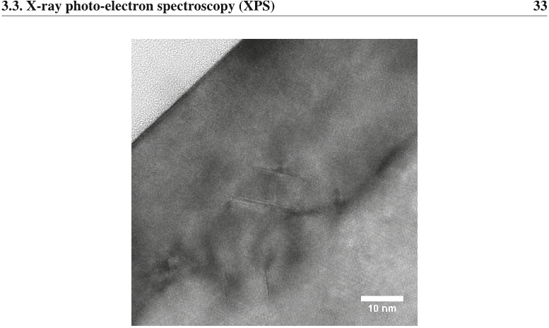 Figure 3.11: Transmition Electron Microscopy (TEM) image showing extended defects in the crystalline lattice of a thin film of SiGe on Si which has been subjected to oxidation at 1000 ◦C.
![Figure 2.6: Diffusivity of Si and Ge in Si1−XGeX as a function of X and modeled following an Arrhenius relation, D = D0exp [−Ea/(kT )]. (a) Activation energies, Ea, for Si and Ge measured in eV. (b) Pre-exponential constant, D0, for Si and Ge measured in cm2/s. (c) Diffusivity of Si in Si1−XGeX for temperatures between 700 and 1100 ◦C. The data is as tabulated by Kube et al [16].](/figures/figure-2-6-diffusivity-of-si-and-ge-in-si1-xgex-as-a-256gx4dj.png) Figure 2.6: Diffusivity of Si and Ge in Si1−XGeX as a function of X and modeled following an Arrhenius relation, D = D0exp [−Ea/(kT )]. (a) Activation energies, Ea, for Si and Ge measured in eV. (b) Pre-exponential constant, D0, for Si and Ge measured in cm2/s. (c) Diffusivity of Si in Si1−XGeX for temperatures between 700 and 1100 ◦C. The data is as tabulated by Kube et al [16].
Figure 2.6: Diffusivity of Si and Ge in Si1−XGeX as a function of X and modeled following an Arrhenius relation, D = D0exp [−Ea/(kT )]. (a) Activation energies, Ea, for Si and Ge measured in eV. (b) Pre-exponential constant, D0, for Si and Ge measured in cm2/s. (c) Diffusivity of Si in Si1−XGeX for temperatures between 700 and 1100 ◦C. The data is as tabulated by Kube et al [16]. Figure 3.6: Angular rotations of a sample in an Eulerian cradle.
![Figure 2.7: Gibbs energies for oxidation of Si and Ge [20].](/figures/figure-2-7-gibbs-energies-for-oxidation-of-si-and-ge-20-whg70kel.png) Figure 2.7: Gibbs energies for oxidation of Si and Ge [20].
Figure 2.7: Gibbs energies for oxidation of Si and Ge [20]. FIG. 8. Oxidation rate ratio, q111=110, versus the oxide thickness of the (111) oriented sample, zox.
 FIG. 9. The oxidation rate ratio between SiGe and Si samples of two orientations, Phkl ¼ ð hklSi 100SiGeÞ=ð 100Si hklSiGeÞ, versus the oxidation rate ratio between SiGe and Si for the (100) orientation, qSiGe=Si ¼ 100SiGe= 100Si . The data are labeled according to the oxidation temperature and the sample orientation (hkl) used to calculate P.
![Figure 2.1: Lattice constant for Si1−XGeX as a function of X [2].](/figures/figure-2-1-lattice-constant-for-si1-xgex-as-a-function-of-x-2rwq6274.png) Figure 2.1: Lattice constant for Si1−XGeX as a function of X [2].
Figure 2.1: Lattice constant for Si1−XGeX as a function of X [2]. Figure 3.15: A schematic of an ion beam implanter modified for Rutherford backscattering spectroscopy (RBS) measurements with a glancing-angle detector geometry.
 FIG. 1. XRD scans of the (004) peaks of (100) oriented SiGe samples after multi-step oxidations with decreasing temperatures. The 2h position for the as-grown sample is marked for reference.
 Figure 4.9: The Ge content in the pile-up layer,Xpu, versus oxidation temperature, T . Values ofXpu were calculated by equation 4.4 using values of zox measured by VASE and values for Em and D0 from table 4.1. Samples include (111), (110), and (100) oriented, MBE grown Si0.8Ge0.2 that have been oxidized at various times, targeting oxide thicknesses of 20, 40, 60, 80, and 100 nm. The data is labeled according to the sample orientation. The lines are linear fits to the data and have intercepts of 1.418, 1.318, 1.361 and slopes of -0.001124, -0.001051, and -0.001087 /◦C for the orientations (111), (110), and (100), respectively.
![Figure 4.8: (a) Activation energies, Ea, for diffusion of Si in SiGe for the (100), (110), and (111) orientations. (b) Diffusivities, D = D0exp [−Ea/(kT )], for Si diffusion in SiGe for three different temperatures. Results from the present work are calculated using Ea = EmXpu +ESi, where ESi = 4.76 eV, and Em and D0 from table 4.1. Results tabulated by Kube et al [15] are also shown.](/figures/figure-4-8-a-activation-energies-ea-for-diffusion-of-si-in-11aoz2t5.png) Figure 4.8: (a) Activation energies, Ea, for diffusion of Si in SiGe for the (100), (110), and (111) orientations. (b) Diffusivities, D = D0exp [−Ea/(kT )], for Si diffusion in SiGe for three different temperatures. Results from the present work are calculated using Ea = EmXpu +ESi, where ESi = 4.76 eV, and Em and D0 from table 4.1. Results tabulated by Kube et al [15] are also shown.
Figure 4.8: (a) Activation energies, Ea, for diffusion of Si in SiGe for the (100), (110), and (111) orientations. (b) Diffusivities, D = D0exp [−Ea/(kT )], for Si diffusion in SiGe for three different temperatures. Results from the present work are calculated using Ea = EmXpu +ESi, where ESi = 4.76 eV, and Em and D0 from table 4.1. Results tabulated by Kube et al [15] are also shown. Table 4.1: Coefficients for the diffusivity of Si in SiGe for different orientations. The activation energy is Ea = EmXpu + ESi, where ESi = 4.76 eV, and D0 is the pre-exponential constant.
 FIG. 6. (Color online) Oxidation rates for Si and SiGe vs the oxide thickness as measured by ellipsometry. Data from the present work is presented along with simulation results. The simulations used the Massoud (Ref. 7) model and published model parameters (Refs. 6 and 7) with the exception of the linear rate constant, B/A, which was determined from the data from the present work.
 Figure 3.7: A schematic describing the diffraction of x-rays by a crystal lattice.
![Figure 2.3: Real, n, and imaginary, k, parts of the complex index of refraction for Si1−XGeX . (a) n and k versus Ge content, X , for 632.8 nm (1.96 eV) light. (b) n and k versus wavelength for Si (X = 0) and Ge (X = 1). [3]](/figures/figure-2-3-real-n-and-imaginary-k-parts-of-the-complex-index-1p5yzgt0.png) Figure 2.3: Real, n, and imaginary, k, parts of the complex index of refraction for Si1−XGeX . (a) n and k versus Ge content, X , for 632.8 nm (1.96 eV) light. (b) n and k versus wavelength for Si (X = 0) and Ge (X = 1). [3]
Figure 2.3: Real, n, and imaginary, k, parts of the complex index of refraction for Si1−XGeX . (a) n and k versus Ge content, X , for 632.8 nm (1.96 eV) light. (b) n and k versus wavelength for Si (X = 0) and Ge (X = 1). [3]![Figure 2.2: Phase diagram for Si1−XGeX [1].](/figures/figure-2-2-phase-diagram-for-si1-xgex-1-35ps6i4o.png) Figure 2.2: Phase diagram for Si1−XGeX [1].
Figure 2.2: Phase diagram for Si1−XGeX [1]. Figure 4.13: Oxide thickness versus oxidation time for samples oxidized at (a) 900, (b) 950, and (c) 1000 ◦C. Data is presented for (111), (110), and (100) oriented, MBE grown Si0.8Ge0.2 and Si control samples. The data is labeled according to the sample type and orientation.
 TABLE II. Oxidation rate ratios, qSiGe=Si, comparing SiGe to Si. The values are averages for all oxidation times for each combination of temperature and orientation.
 FIG. 7. The Ge content in the pile-up layer, Xpu, versus oxide thickness, zox. The lines are for visual guidance only.
 TABLE III. Oxidation rate ratios, q110=100; q111=100, and q111=110, for the stated orientations. The values are averages for Si or SiGe (as indicated) for the five oxidation times used at each temperature.
 Figure 3.10: XRD reciprocal space maps of the (-1-13), (004), and (113) peaks of a (100) oriented sample with an 80 nm epitaxial layer of Si0.8Ge0.2 on a Si substrate. The epitaxial layer of SiGe has a slight tilt with respect to the substrate.
![FIG. 10. (Color online) A plot of the scaled ratio of doses from Eq. (10) vs oxide thickness. Here, B¼ {1 þ (1 Xpileup)X/[Xpileup(1 X)]}.](/figures/fig-10-color-online-a-plot-of-the-scaled-ratio-of-doses-from-31xxcv89.png) FIG. 10. (Color online) A plot of the scaled ratio of doses from Eq. (10) vs oxide thickness. Here, B¼ {1 þ (1 Xpileup)X/[Xpileup(1 X)]}.
FIG. 10. (Color online) A plot of the scaled ratio of doses from Eq. (10) vs oxide thickness. Here, B¼ {1 þ (1 Xpileup)X/[Xpileup(1 X)]}.![Figure 3.2: Ellipsometry models using (a) a single layer and (b) two layers. After figure 5-24 of [3].](/figures/figure-3-2-ellipsometry-models-using-a-a-single-layer-and-b-31ujoo5s.png) Figure 3.2: Ellipsometry models using (a) a single layer and (b) two layers. After figure 5-24 of [3].
Figure 3.2: Ellipsometry models using (a) a single layer and (b) two layers. After figure 5-24 of [3]. Figure 3.3: Color maps for χ2 values calculated with a two layer model and a range of values for two unknowns. Red areas represent combinations of the two unknowns with large χ2 values, while blue areas represent lower χ2 values. The color maps demonstrate that a large number of minima can be generated for various combinations of values for the two unknowns without producing a unique minimum χ2 value during analysis of ellipsometry data.
 Figure 3.14: XPS spectrum of oxidized SiGe with Ge incorporated into the oxide. The spectrum shows the binding energies of emitted electrons for silicon (Si), germanium (Ge), and oxygen (O.) The peaks due to photo-electrons are marked by the core energy levels from which the electrons are emitted, while the Auger emission peaks are labeled according to the levels involved in the Auger transitions.
![Figure 2.4: Minimum energy band gap for Si1−XGeX as a function of X [7, 8]. Curves are shown for both relaxed Si1−XGeX and strained layers of Si1−XGeX on a Si(100) substrate.](/figures/figure-2-4-minimum-energy-band-gap-for-si1-xgex-as-a-3rvkfejb.png) Figure 2.4: Minimum energy band gap for Si1−XGeX as a function of X [7, 8]. Curves are shown for both relaxed Si1−XGeX and strained layers of Si1−XGeX on a Si(100) substrate.
Figure 2.4: Minimum energy band gap for Si1−XGeX as a function of X [7, 8]. Curves are shown for both relaxed Si1−XGeX and strained layers of Si1−XGeX on a Si(100) substrate.![Figure 3.13: XPS and Auger transitions between energy levels. After figures 10.8 and 10.33 of [2].](/figures/figure-3-13-xps-and-auger-transitions-between-energy-levels-132v9upw.png) Figure 3.13: XPS and Auger transitions between energy levels. After figures 10.8 and 10.33 of [2].
Figure 3.13: XPS and Auger transitions between energy levels. After figures 10.8 and 10.33 of [2].![Figure 4.7: Critical layer thickness for epitaxial Si1−XGeX on a Si substrate as a function of X . Curves shown follow predictions by Matthews and Blakeslee [25] and People and Bean [26]. Pile-up thicknesses (calculated with equation 4.5) as a function of Ge content in the pile-up layer for (a) a 50 nm oxide and different initial layer Ge contents, and (b) for a Si0.99Ge0.01 initial layer and different oxide thicknesses. The axis showing Ge content in the pile-up corresponds directly to the oxidation temperature axis (Xpu = 1.361− ( 1.087× 10⁻³ × T ) /◦C). Data shown is for the (100) orientation.](/figures/figure-4-7-critical-layer-thickness-for-epitaxial-si1-xgex-ejye01a5.png) Figure 4.7: Critical layer thickness for epitaxial Si1−XGeX on a Si substrate as a function of X . Curves shown follow predictions by Matthews and Blakeslee [25] and People and Bean [26]. Pile-up thicknesses (calculated with equation 4.5) as a function of Ge content in the pile-up layer for (a) a 50 nm oxide and different initial layer Ge contents, and (b) for a Si0.99Ge0.01 initial layer and different oxide thicknesses. The axis showing Ge content in the pile-up corresponds directly to the oxidation temperature axis (Xpu = 1.361− ( 1.087× 10⁻³ × T ) /◦C). Data shown is for the (100) orientation.
Figure 4.7: Critical layer thickness for epitaxial Si1−XGeX on a Si substrate as a function of X . Curves shown follow predictions by Matthews and Blakeslee [25] and People and Bean [26]. Pile-up thicknesses (calculated with equation 4.5) as a function of Ge content in the pile-up layer for (a) a 50 nm oxide and different initial layer Ge contents, and (b) for a Si0.99Ge0.01 initial layer and different oxide thicknesses. The axis showing Ge content in the pile-up corresponds directly to the oxidation temperature axis (Xpu = 1.361− ( 1.087× 10⁻³ × T ) /◦C). Data shown is for the (100) orientation. Figure 4.14: (a) Average values of ρSiGe/Si from table 4.3 versus oxidation temperature. The data is separated by crystallographic orientation. (b) Values of ρSiGe/Si versus Xpu as measured by XRD.
 Figure 4.3: The pile-up layer thickness, zpu, as measured by XRD compared to the values measured by RBS. (a) The solid diagonal line is drawn as a visual guide to indicate where x = y. The dashed lines represent ±σ = 48Å. (b) The solid line is the linear regression to the data (bR = 57Å, mR = 0.72, rR = 0.70) and the dashed lines represent ±σSE = 33Å
 Figure 4.2: The pile-up layer thickness, zpu, as measured by XRD compared to the values measured by VASE. (a) The solid diagonal line is drawn as a visual guide to indicate where x = y. The dashed lines represent ±σ = 37Å. (b) The solid line is the linear regression to the data (bR = −6Å, mR = 0.93, rR = 0.92) and the dashed lines represent ±σSE = 34Å
 FIG. 4. (Color online) Ge concentration in the pile-up layer of SiGe samples plotted against oxidation temperature. Data measured by XRD is presented alongside simulation results. The measured data is for samples with initial layers of both 15% and 20% Ge (presented as a single series) while the simulated points are for initial SiGe layers of 20% and 5% Ge and labeled accordingly. Simulated results are presented for three oxide thicknesses and labeled accordingly. The lines connecting the simulated points are for visual guidance only.
 FIG. 5. (Color online) Ge concentration in the pile-up layer of SiGe samples plotted against oxidation temperature. Data measured by XRD is presented alongside modeled data determined by Eq. (3), using oxide thicknesses determined by ellipsometry. The linear fit to the measured data was used to determine Eq. (1). The coefficients of the activation energy and preexponential for the diffusivity of Si in SiGe were determined by matching the linear regressions for the modeled and measured data. The measured and modeled data is for samples with initial layers of both 15% and 20% Ge (presented as a single series.)
![Figure 3.8: Bragg diffraction peaks for a crystal with a diamond structure that has a (100) oriented surface plotted in Q space. The peaks that are forbidden due to instrument or sample geometry and due to the sample’s crystal structure are excluded. After figure 7.16 in [10].](/figures/figure-3-8-bragg-diffraction-peaks-for-a-crystal-with-a-2cts76iy.png) Figure 3.8: Bragg diffraction peaks for a crystal with a diamond structure that has a (100) oriented surface plotted in Q space. The peaks that are forbidden due to instrument or sample geometry and due to the sample’s crystal structure are excluded. After figure 7.16 in [10].
Figure 3.8: Bragg diffraction peaks for a crystal with a diamond structure that has a (100) oriented surface plotted in Q space. The peaks that are forbidden due to instrument or sample geometry and due to the sample’s crystal structure are excluded. After figure 7.16 in [10]. FIG. 8. Oxidation rate ratio, q111=110, versus the oxide thickness of the (111) oriented sample, zox.
 FIG. 7. The Ge content in the pile-up layer, Xpu, versus oxide thickness, zox. The lines are for visual guidance only.
 Table 4.2: Values for ρ110/100, ρ111/100 and ρ111/110, where ρ is the ratio of oxidation rates for the given orientations. The values shown are the average values for Si or SiGe (as indicated) for the five oxidation times used at each oxidation temperature.
 Table 4.3: Values for ρSiGe/Si, where ρ is the ratio of oxidation rates of SiGe and Si samples. The values shown are the averages of values for all oxidation times for any given temperature (in ◦C) and orientation used in the present work.
![Figure 3.4: The (a) real and (b) imaginary components of the indices of refraction for Si, Si0.70Ge0.30, and Si0.35Ge0.65. The data is extracted from the CompleteEASE software by J.A. Woollam Co. [4] following data presented in [6] and [7].](/figures/figure-3-4-the-a-real-and-b-imaginary-components-of-the-33j4jtp4.png) Figure 3.4: The (a) real and (b) imaginary components of the indices of refraction for Si, Si0.70Ge0.30, and Si0.35Ge0.65. The data is extracted from the CompleteEASE software by J.A. Woollam Co. [4] following data presented in [6] and [7].
Figure 3.4: The (a) real and (b) imaginary components of the indices of refraction for Si, Si0.70Ge0.30, and Si0.35Ge0.65. The data is extracted from the CompleteEASE software by J.A. Woollam Co. [4] following data presented in [6] and [7]. FIG. 2. (Color online) Ge concentration in the pile-up layer plotted against oxide thickness for samples oxidized at various temperatures and labeled accordingly. Ge concentrations are determined by XRD; oxide thicknesses are determined by ellipsometry. The lines connecting the measured data points are for visual guidance only. FIG. 3. (Color online) Pile-up layer thicknesses of Si0.85Ge0.15 and Si0.8Ge0.2 samples plotted against oxide thickness. The pile-up layer thicknesses are determined by XRD; oxide thicknesses are determined by ellipsometry. Linear fits to the measured data are included to aid in visual interpretation of the data.
 TABLE I. Parameters for diffusivity of Si in SiGe for different orientations.
 FIG. 6. (Color online) Oxidation rates for Si and SiGe vs the oxide thickness as measured by ellipsometry. Data from the present work is presented along with simulation results. The simulations used the Massoud (Ref. 7) model and published model parameters (Refs. 6 and 7) with the exception of the linear rate constant, B/A, which was determined from the data from the present work.
 Figure 4.12: The Ge content in the pile-up layer, Xpu, versus oxide thickness, zox. Values of Xpu were calculated by equation 4.4 using values of zox measured by VASE and values for Em and D0 from table 4.1. Samples include (111), (110), and (100) oriented, MBE grown Si0.8Ge0.2 that have been oxidized at 900, 950, and 1000 ◦C. The data is labeled according to the sample orientation and oxidation temperature. The lines connecting data points are for visual guidance only.
![Figure 3.1: A schematic of the AutoEL-II ellipsometer by Rudolph Research showing basic functional components. After drawing number D7905-8 of [3].](/figures/figure-3-1-a-schematic-of-the-autoel-ii-ellipsometer-by-3ffakscc.png) Figure 3.1: A schematic of the AutoEL-II ellipsometer by Rudolph Research showing basic functional components. After drawing number D7905-8 of [3].
Figure 3.1: A schematic of the AutoEL-II ellipsometer by Rudolph Research showing basic functional components. After drawing number D7905-8 of [3]. Figure 4.15: Oxidation rate ratio, ρSiGe/Si, versus the oxide thickness, zox, of the SiGe sample. The oxidation rate ratio is calculated as ρSiGe/Si = νhklSiGe/ν hkl Si , where ν is the oxidation rate and hkl is one of the three crystallographic orientations in the the present work, (111), (110), or (100). The data is labeled according to the oxidation temperature.
 Figure 3.12: A schematic of an x-ray photo-electron spectroscopy (XPS) instrument.
 FIG. 9. The oxidation rate ratio between SiGe and Si samples of two orientations, Phkl ¼ ð hklSi 100SiGeÞ=ð 100Si hklSiGeÞ, versus the oxidation rate ratio between SiGe and Si for the (100) orientation, qSiGe=Si ¼ 100SiGe= 100Si . The data are labeled according to the oxidation temperature and the sample orientation (hkl) used to calculate P.
 Figure 3.9: XRD 2θ-ω scans of samples with 80 nm epitaxial layers of Si1−XGeX on a Si substrate. The (004) peak is measured for (100) oriented material, the (333) peak for (111) material, and the (022) and (044) peaks for (110) material.
 Figure 4.4: The oxide layer thickness, zox, as measured by RBS compared to the values measured by VASE. (a) The solid diagonal line is drawn as a visual guide to indicate where x = y. The dashed lines represent ±σ = 71Å. (b) The solid line is the linear regression to the data (bR = 25Å, mR = 0.82, rR = 0.91) and the dashed lines represent ±σSE = 46Å
![Figure 2.5: Critical layer thickness for epitaxial Si1−XGeX on a Si substrate as a function of X . Curves shown follow predictions by Matthews and Blakeslee [13] and People and Bean [14]. The predictions by People and Bean may fall within a region of metastability such that defects and relaxation will develop over time [4].](/figures/figure-2-5-critical-layer-thickness-for-epitaxial-si1-xgex-gbhasqww.png) Figure 2.5: Critical layer thickness for epitaxial Si1−XGeX on a Si substrate as a function of X . Curves shown follow predictions by Matthews and Blakeslee [13] and People and Bean [14]. The predictions by People and Bean may fall within a region of metastability such that defects and relaxation will develop over time [4].
Figure 2.5: Critical layer thickness for epitaxial Si1−XGeX on a Si substrate as a function of X . Curves shown follow predictions by Matthews and Blakeslee [13] and People and Bean [14]. The predictions by People and Bean may fall within a region of metastability such that defects and relaxation will develop over time [4]. Figure 4.16: Oxidation rate ratio, ρ111/110, versus the oxide thickness, zox, of the (111) oriented sample. The oxidation rate ratio is calculated as ρ111/110 = ν111/ν110, where νhkl is the oxidation rate. The data is labeled according to the sample type, SiGe or Si.
![Figure 4.6: Oxide and pile-up layer thicknesses; comparison of calculated and measured values. (a) & (b) Oxide thickness, zox, calculated with equation 4.5 versus VASE measurements. The calculated values use zpu, Xpu, and X as measured by XRD. (c) & (d) Pile-up layer thickness, zpu, calculated with equation 4.5 versus XRD measurements. The calculated values use zox measured by VASE while Xpu and X are measured by XRD. The atomic density of the pile-up layer, Npu, follows data presented by Dismukes et al [16]. (a) & (c) The solid line is a visual guide showing where x = y. The dashed lines represent ±σ. (b) & (d) The solid line is the linear regression to the data and the dashed lines represent ±σSE. (a) & (b) σ = 148Å, bR = −145Å,mR = 1.53, rR = 0.96, σSE = 85Å (c) & (d) σ = 44Å, bR = 20Å,mR = 0.62, rR = 0.98, σSE = 8Å](/figures/figure-4-6-oxide-and-pile-up-layer-thicknesses-comparison-of-1pebucxx.png) Figure 4.6: Oxide and pile-up layer thicknesses; comparison of calculated and measured values. (a) & (b) Oxide thickness, zox, calculated with equation 4.5 versus VASE measurements. The calculated values use zpu, Xpu, and X as measured by XRD. (c) & (d) Pile-up layer thickness, zpu, calculated with equation 4.5 versus XRD measurements. The calculated values use zox measured by VASE while Xpu and X are measured by XRD. The atomic density of the pile-up layer, Npu, follows data presented by Dismukes et al [16]. (a) & (c) The solid line is a visual guide showing where x = y. The dashed lines represent ±σ. (b) & (d) The solid line is the linear regression to the data and the dashed lines represent ±σSE. (a) & (b) σ = 148Å, bR = −145Å,mR = 1.53, rR = 0.96, σSE = 85Å (c) & (d) σ = 44Å, bR = 20Å,mR = 0.62, rR = 0.98, σSE = 8Å
Figure 4.6: Oxide and pile-up layer thicknesses; comparison of calculated and measured values. (a) & (b) Oxide thickness, zox, calculated with equation 4.5 versus VASE measurements. The calculated values use zpu, Xpu, and X as measured by XRD. (c) & (d) Pile-up layer thickness, zpu, calculated with equation 4.5 versus XRD measurements. The calculated values use zox measured by VASE while Xpu and X are measured by XRD. The atomic density of the pile-up layer, Npu, follows data presented by Dismukes et al [16]. (a) & (c) The solid line is a visual guide showing where x = y. The dashed lines represent ±σ. (b) & (d) The solid line is the linear regression to the data and the dashed lines represent ±σSE. (a) & (b) σ = 148Å, bR = −145Å,mR = 1.53, rR = 0.96, σSE = 85Å (c) & (d) σ = 44Å, bR = 20Å,mR = 0.62, rR = 0.98, σSE = 8Å Figure 3.5: A schematic of an x-ray diffraction (XRD) instrument.
 Figure 3.16: Two example spectra measured by Rutherford backscattering spectroscopy (RBS). The samples were thin films of SiGe on a Si substrate, one of the samples was oxidized to enhance the Ge content of the SiGe layer.
 Figure 4.10: Energy Filtered Transmission Electron Microscopy (EFTEM) mapping of the Ge content in samples subjected to multiple oxidations. (a) Si0.8Ge0.2 oxidized at 1000 ◦C and then at 900 ◦C. (b) Si0.8Ge0.2 oxidized at 1000 ◦C and then again at 1000 ◦C. Discussion and analysis of the XRD data for these samples is presented in chapter 6.4.
![Figure 4.11: Phase diagram for Si1−XGeX as a function of X [27]. The Ge content in the pile-up as a function of oxidation temperature for the (111), (110), and (100) orientations is also shown. For any given oxidation temperature the Ge content in the pile-up will be limited such that the pile-up layer remains solid (i.e. the SiGe will not melt during oxidation).](/figures/figure-4-11-phase-diagram-for-si1-xgex-as-a-function-of-x-27-23nh8r1r.png) Figure 4.11: Phase diagram for Si1−XGeX as a function of X [27]. The Ge content in the pile-up as a function of oxidation temperature for the (111), (110), and (100) orientations is also shown. For any given oxidation temperature the Ge content in the pile-up will be limited such that the pile-up layer remains solid (i.e. the SiGe will not melt during oxidation).
Figure 4.11: Phase diagram for Si1−XGeX as a function of X [27]. The Ge content in the pile-up as a function of oxidation temperature for the (111), (110), and (100) orientations is also shown. For any given oxidation temperature the Ge content in the pile-up will be limited such that the pile-up layer remains solid (i.e. the SiGe will not melt during oxidation). FIG. 3. Oxide thickness versus oxidation time at (a) 900, (b) 950, and (c) 1000 C. The data are for (111), (110), and (100) oriented Si0:8Ge0:2 and Si.

![Figure 5.1: Gibbs energies for oxidation of Si, Ge, and Sn [6].](/figures/figure-5-1-gibbs-energies-for-oxidation-of-si-ge-and-sn-6-2r8beopl.webp)


![Figure 2.6: Diffusivity of Si and Ge in Si1−XGeX as a function of X and modeled following an Arrhenius relation, D = D0exp [−Ea/(kT )]. (a) Activation energies, Ea, for Si and Ge measured in eV. (b) Pre-exponential constant, D0, for Si and Ge measured in cm2/s. (c) Diffusivity of Si in Si1−XGeX for temperatures between 700 and 1100 ◦C. The data is as tabulated by Kube et al [16].](/figures/figure-2-6-diffusivity-of-si-and-ge-in-si1-xgex-as-a-256gx4dj.webp)

![Figure 2.7: Gibbs energies for oxidation of Si and Ge [20].](/figures/figure-2-7-gibbs-energies-for-oxidation-of-si-and-ge-20-whg70kel.webp)


![Figure 2.1: Lattice constant for Si1−XGeX as a function of X [2].](/figures/figure-2-1-lattice-constant-for-si1-xgex-as-a-function-of-x-2rwq6274.webp)


![Figure 4.8: (a) Activation energies, Ea, for diffusion of Si in SiGe for the (100), (110), and (111) orientations. (b) Diffusivities, D = D0exp [−Ea/(kT )], for Si diffusion in SiGe for three different temperatures. Results from the present work are calculated using Ea = EmXpu +ESi, where ESi = 4.76 eV, and Em and D0 from table 4.1. Results tabulated by Kube et al [15] are also shown.](/figures/figure-4-8-a-activation-energies-ea-for-diffusion-of-si-in-11aoz2t5.webp)


![Figure 2.3: Real, n, and imaginary, k, parts of the complex index of refraction for Si1−XGeX . (a) n and k versus Ge content, X , for 632.8 nm (1.96 eV) light. (b) n and k versus wavelength for Si (X = 0) and Ge (X = 1). [3]](/figures/figure-2-3-real-n-and-imaginary-k-parts-of-the-complex-index-1p5yzgt0.webp)
![Figure 2.2: Phase diagram for Si1−XGeX [1].](/figures/figure-2-2-phase-diagram-for-si1-xgex-1-35ps6i4o.webp)


![FIG. 10. (Color online) A plot of the scaled ratio of doses from Eq. (10) vs oxide thickness. Here, B¼ {1 þ (1 Xpileup)X/[Xpileup(1 X)]}.](/figures/fig-10-color-online-a-plot-of-the-scaled-ratio-of-doses-from-31xxcv89.webp)
![Figure 3.2: Ellipsometry models using (a) a single layer and (b) two layers. After figure 5-24 of [3].](/figures/figure-3-2-ellipsometry-models-using-a-a-single-layer-and-b-31ujoo5s.webp)


![Figure 2.4: Minimum energy band gap for Si1−XGeX as a function of X [7, 8]. Curves are shown for both relaxed Si1−XGeX and strained layers of Si1−XGeX on a Si(100) substrate.](/figures/figure-2-4-minimum-energy-band-gap-for-si1-xgex-as-a-3rvkfejb.webp)
![Figure 3.13: XPS and Auger transitions between energy levels. After figures 10.8 and 10.33 of [2].](/figures/figure-3-13-xps-and-auger-transitions-between-energy-levels-132v9upw.webp)
![Figure 4.7: Critical layer thickness for epitaxial Si1−XGeX on a Si substrate as a function of X . Curves shown follow predictions by Matthews and Blakeslee [25] and People and Bean [26]. Pile-up thicknesses (calculated with equation 4.5) as a function of Ge content in the pile-up layer for (a) a 50 nm oxide and different initial layer Ge contents, and (b) for a Si0.99Ge0.01 initial layer and different oxide thicknesses. The axis showing Ge content in the pile-up corresponds directly to the oxidation temperature axis (Xpu = 1.361− ( 1.087× 10⁻³ × T ) /◦C). Data shown is for the (100) orientation.](/figures/figure-4-7-critical-layer-thickness-for-epitaxial-si1-xgex-ejye01a5.webp)


![Figure 3.8: Bragg diffraction peaks for a crystal with a diamond structure that has a (100) oriented surface plotted in Q space. The peaks that are forbidden due to instrument or sample geometry and due to the sample’s crystal structure are excluded. After figure 7.16 in [10].](/figures/figure-3-8-bragg-diffraction-peaks-for-a-crystal-with-a-2cts76iy.webp)


![Figure 3.4: The (a) real and (b) imaginary components of the indices of refraction for Si, Si0.70Ge0.30, and Si0.35Ge0.65. The data is extracted from the CompleteEASE software by J.A. Woollam Co. [4] following data presented in [6] and [7].](/figures/figure-3-4-the-a-real-and-b-imaginary-components-of-the-33j4jtp4.webp)


![Figure 3.1: A schematic of the AutoEL-II ellipsometer by Rudolph Research showing basic functional components. After drawing number D7905-8 of [3].](/figures/figure-3-1-a-schematic-of-the-autoel-ii-ellipsometer-by-3ffakscc.webp)


![Figure 2.5: Critical layer thickness for epitaxial Si1−XGeX on a Si substrate as a function of X . Curves shown follow predictions by Matthews and Blakeslee [13] and People and Bean [14]. The predictions by People and Bean may fall within a region of metastability such that defects and relaxation will develop over time [4].](/figures/figure-2-5-critical-layer-thickness-for-epitaxial-si1-xgex-gbhasqww.webp)

![Figure 4.6: Oxide and pile-up layer thicknesses; comparison of calculated and measured values. (a) & (b) Oxide thickness, zox, calculated with equation 4.5 versus VASE measurements. The calculated values use zpu, Xpu, and X as measured by XRD. (c) & (d) Pile-up layer thickness, zpu, calculated with equation 4.5 versus XRD measurements. The calculated values use zox measured by VASE while Xpu and X are measured by XRD. The atomic density of the pile-up layer, Npu, follows data presented by Dismukes et al [16]. (a) & (c) The solid line is a visual guide showing where x = y. The dashed lines represent ±σ. (b) & (d) The solid line is the linear regression to the data and the dashed lines represent ±σSE. (a) & (b) σ = 148Å, bR = −145Å,mR = 1.53, rR = 0.96, σSE = 85Å (c) & (d) σ = 44Å, bR = 20Å,mR = 0.62, rR = 0.98, σSE = 8Å](/figures/figure-4-6-oxide-and-pile-up-layer-thicknesses-comparison-of-1pebucxx.webp)


![Figure 4.11: Phase diagram for Si1−XGeX as a function of X [27]. The Ge content in the pile-up as a function of oxidation temperature for the (111), (110), and (100) orientations is also shown. For any given oxidation temperature the Ge content in the pile-up will be limited such that the pile-up layer remains solid (i.e. the SiGe will not melt during oxidation).](/figures/figure-4-11-phase-diagram-for-si1-xgex-as-a-function-of-x-27-23nh8r1r.webp)
