
All figures (5)
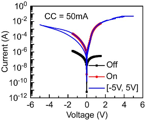
Fig. 4. Coexistence of WORM memory and RRAM in one cell. 
Fig. 5. (a) C-AFM image of the surface of ZnO thin film. (b) Spot of 5 nm corresponding to the black square area in (a). (c) Typical SEM images of blown-off and bubble areas on top of contact for ON-state WORM memory. (d) Magnified images of the bubble in the rectangular area of (c). 
Fig. 1. (a) Switching characteristics of the WORM memory. (Black squares) Current–voltage (I–V ) characteristic of the WORM memory before writing (OFF state). (Red circles) Data for the WORM memory after writing (ON state). (Bottom right inset) Device structure of the WORM memory. (Top right inset) I–V characteristic for the writing process. (Left inset) Probability of the resistance ratio between OFF and ON states for 100 devices of 30 μm × 30 μm. (b) Dependence of ON- and OFF-state resistances and writing power on current compliance during the writing process. ![Fig. 3. Dependence of resistance for ON and OFF states on the area of the device. (Inset) Cumulative probability of writing voltage for different device areas [(noted as “1” in the inset) 30 × 30, (2) 50 × 50, (3) 100 × 100, (4) 200 × 200, (5) 400 × 400, and (6) 600 × 600 μm2].](/figures/fig-3-dependence-of-resistance-for-on-and-off-states-on-the-sh7c3p46.png)
Fig. 3. Dependence of resistance for ON and OFF states on the area of the device. (Inset) Cumulative probability of writing voltage for different device areas [(noted as “1” in the inset) 30 × 30, (2) 50 × 50, (3) 100 × 100, (4) 200 × 200, (5) 400 × 400, and (6) 600 × 600 μm2]. 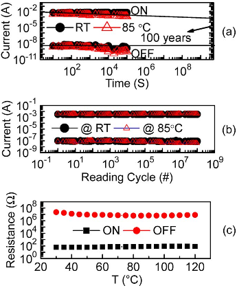
Fig. 2. (a) Retention and (b) endurance characteristics of the ZnO WORM memory device in the ON and OFF states at a read voltage of 1.0 V. (c) Dependence of resistance on measurement temperature.


![Fig. 3. Dependence of resistance for ON and OFF states on the area of the device. (Inset) Cumulative probability of writing voltage for different device areas [(noted as “1” in the inset) 30 × 30, (2) 50 × 50, (3) 100 × 100, (4) 200 × 200, (5) 400 × 400, and (6) 600 × 600 μm2].](/figures/fig-3-dependence-of-resistance-for-on-and-off-states-on-the-sh7c3p46.webp)
