Residual strain in the Nb
3
Sn 11 T dipole magnet coils for
HL-LHC
C. Scheuerlein
1
, M. Di Michiel
2
, M. Hofmann
3
, M. Lorentzon
1
, F. Lackner
1
, R. Flükiger
1
, F. Savary
1
,
L. Bottura
1
1
European Organization for Nuclear Research (CERN), CH 1211 Geneva 23, Switzerland
2
European Synchrotron Radiation Facility, 6 rue Jules Horowitz, F-38000 Grenoble, France
3
Forschungsneutronenquelle Heinz Maier-Leibnitz (FRM II), TU München, D-85748 Garching, Germany
Abstract. Nb
3
Sn magnets are presently build for the HL-LHC accelerator upgrade and are developed
for the Future Circular Collider (FCC) study. The knowledge of the Nb
3
Sn strain state distribution
in these magnets is required in order to predict their ultimate performance limit. We have measured
the Nb
3
Sn residual strain distribution in an 11 T dipole accelerator magnet coil. Ambient temperature
Nb
3
Sn strain maps across 11 T dipole coil cross sections were acquired by means of fast high energy
synchrotron X-ray diffraction. Using complementary neutron diffraction measurements the Nb
3
Sn
residual strain and stress was measured in the four largest conductor blocks of a massive 11 T dipole
coil segment.
1. Introduction
The next generation superconducting accelerator magnets [
1
] presently built for the LHC High
Luminosity upgrade (HL-LHC) [
2
], and developed for the Future Circular Collider (FCC) project, is based
on Nb
3
Sn superconductors. The superconducting properties of Nb
3
Sn are strain sensitive, and the reversible
strain dependence of the critical current density (J
c
) is commonly ascribed to elastic Nb
3
Sn lattice distortions
[
3
,
4
,
5
]. When the externally applied load to the coil exceeds a critical value, crack formation in the Nb
3
Sn
filaments causes an irreversible J
c
degradation [
6
]. Thus, a precise knowledge of the Nb
3
Sn strain and stress
state in the conductor is required in order to predict the ultimate Nb
3
Sn performance limit in magnets and
the critical stress levels not to be exceeded during magnet assembly and operation.
The Nb
3
Sn strain state in a magnet coil may be influenced by mechanical material properties of the
conductor constituents, by friction coefficients between different materials pairs, by cabling, coil winding
and Nb
3
Sn reaction processes, by the collaring and magnet assembly at ambient temperature and finally by
thermal and powering cycles of the magnets during operation.
The first Nb
3
Sn lattice spacing measurements reported have been performed using 8.04 keV Cu K
α
X-rays provided by commonly used laboratory diffractometers. Since their penetration depth is not
sufficient to reach the Nb
3
Sn filaments in the wire matrix the measurements were performed either on thin
tapes or on wires where the outer sheath was removed [
7
,
8
].
Modern high energy synchrotron beamlines provide a very high flux of X-rays with energies
>100 keV, exceeding the neutron flux of the most powerful neutron sources by several orders of magnitude.
This enables the acquisition of diffraction patterns of Nb
3
Sn wires with excellent signal to noise ratio within
seconds [
9
]. This makes high energy synchrotron X-ray diffraction an excellent tool for in situ monitoring
of the variations of the strain state in composite superconductors submitted to mechanical loads [
10
], and it
enables the acquisition of strain maps with high spatial resolution.

The penetration depth of high energy photons in the highly absorbing metallic Nb
3
Sn
superconductors is limited to a few millimeters. Neutron diffraction measurements have also been applied
to study the strain state in Nb
3
Sn wires [
11
], and they are particularly well suited to study samples with
relatively large sample volume, like the ITER Nb
3
Sn central solenoid cable [
12
].
In this article we report for the first time a direct observation of the residual strain distribution in a
reacted Nb
3
Sn magnet coil, based on high energy synchrotron X-ray diffraction and neutron diffraction
measurements.
2. Experimental
2.1 The 11 T dipole Nb
3
Sn coil samples
The 11 T dipole [
13
] magnet coils are wound from unreacted Nb
3
Sn Rutherford cables [
14
,
15
]
consisting of RRP type wires [
16
], a 25 µm-thick stainless steel core, and a 0.15 mm-thick cable insulation
made of a Mica tape and S2/E-glass fiber. After the Nb
3
Sn reaction heat treatment with a peak temperature
of typically 650 °C, the void space in the reacted coils is filled with epoxy resin CTD-101K from Composite
Technology Development [
17
], in order to improve the electromechanical coil properties.
2.2 High energy synchrotron X-ray diffraction
Synchrotron X-ray diffraction measurements were carried out at the new ID15A High Energy
Scattering Beamline of the European Synchrotron (ESRF) in transmission geometry (Figure 1(a)) using a
150 keV monochromatic X-ray beam with a bandwidth of ±300 eV. The X-ray beam had a cross section of
0.2 mm × 0.2 mm. Diffracted X-rays were recorded on a Pilatus3 X CdTe 2M detector, with a sample to
detector distance of 1963.6 mm. For the calibration of the photon energy and the sample to detector distance
a Cerium Dioxide (CeO
2
) reference powder has been used. The samples consist of 3 mm thick coil slices
extracted from the Nb
3
Sn 11 T dipole coil #107 that previously had been cold tested in a short model magnet.
The calculated transmissions of 150 keV photons through a 3 mm thick layer of Nb
3
Sn and Cu are 23% and
55%, respectively. For strain mapping, slices have been cut in the center of the straight coil part and in the
coil pole end. Figure 1(b) shows a slice from the straight coil part mounted on the goniometer of the ID15A
sample stage.
Figure 1: (a) Sketch of ID15A test configuration. (b) 11 T coil slice on the goniometer of the ID15A sample stage.
Entire diffraction rings were recorded in such a way that a d-spacing range from 1.40 to 2.65 Å
could be analyzed. The two-dimensional diffraction patterns were caked in 36 circular sectors, each one of
them being radially integrated in order to measure lattice parameters from the crystalline planes oriented
both in the radial and the hoop direction.
(b)

The sample was aligned parallel to the X-ray beam (Ω = 90º) and centered on the rotation axis. In
order to achieve a strain resolution of ~0.01% the sample-detector distance needs to be controlled within
~200 µm. During the experiment the wires in the 3 mm thick coil slice were not aligned parallel to the beam,
but were tilted by the cable transposition pitch (about 0.45 mm over the 3 mm coil segment thickness). Since
this wire tilt affects the wire position where the 200 × 200 μm
2
beam interacts the sample-to-detector
distance varies across the 3 mm-thick coil segment. In order to get sufficiently accurate absolute strain
results, diffraction scans across the same sample were always acquired two times, at Ω = 0 º and at Ω =
180º. Absolute d-spacing values were obtained by overlaying and averaging the Ω = 0 º and Ω = 180º data
points. This procedure also eliminates uncertainties due to small sample bending or thickness variations.
The strain resolution of the experiment is better than 0.01% (equivalent to 0.1 detector pixels).
About 100’000 diffractograms were acquired for the strain mapping in the two coil cross sections
presented in this article. Single Nb
3
Sn (321) and Cu (200) peaks have been fitted with Pseudo Voigt
functions and peak position (d-spacing), peak area and peak width were determined from these fits. Multiple
peak fitting has been performed on selected diffractograms. The main Nb (100) peak is not present in this
configuration (beam parallel to wire drawing axis) because of the strong Nb texture [
18
].
2.3 Neutron diffraction
Neutron diffraction experiments were performed at the Stress-Spec diffractometer at the FRM II
neutron source of the Heinz Maier-Leibnitz Zentrum MLZ [
19
]. Because of the comparatively deep
penetration of the neutron beam, diffraction measurements could be performed in the center of a massive
4 cm-thick 11 T coil #107 segment, and the Nb
3
Sn lattice parameter was measured in the center of the four
largest conductor blocks in axial, radial and hoop directions (Figure 2).
Figure 2: 4 cm-long segment of 11 T short model coil #107 mounted on the Stress-Spec sample stage in axial test
configuration. The gauge volume centre positions in radial and hoop position are labelled.
A bent Si (400) monochromator provides a neutron beam with a wavelength of λ=1.672 ±0.003 Å
as determined by refinement of the diffractogram of a Si standard powder with FullProf software. The
refinement also revealed a 2Ɵ offset: + 0.232°. The nominal gauge volume 5×5×5 mm
3
is defined by a
5×5 mm
2
slit that shape the beam and by a radial collimator in front of the detector.
A 2Ɵ range 70.5°<2Ɵ<83.5° was recorded, and Nb
3
Sn (321) and Cu (220) reflections were fitted
by Gaussian functions. Prior to peak fitting the diffratcograms were corrected for the detector efficiency
using incoherent scattering from a Vanadium scan. The acquisition time for one diffractogram in radial and
axial directions was 1 hour and in hoop direction 3 hours, respectively.

For measurements at <10 K the sample was mounted on the cold head of a Cryocooler Sumitomo
SRDK 101D with a M6 threaded rod. The temperature regulation was performed using a Cernox
temperature sensor connected to the cryocooler cold head. The sample temperature was measured with a
Cernox sensor screwed to the opposed sample surface.
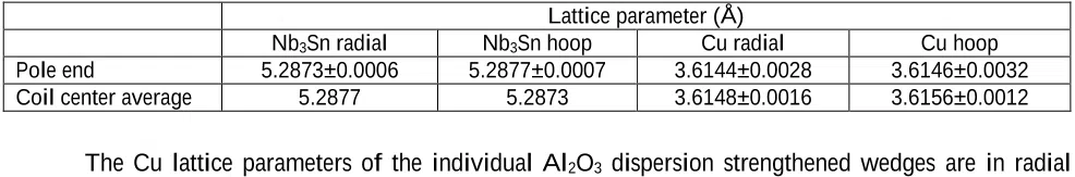
3. Results
3.1 Nb
3
Sn and Cu lattice parameters in extracted wires
In order to measure the Nb
3
Sn and Cu lattice parameters at room temperature (RT) without stress
exerted by the surrounding coil, individual wires were extracted from coil #107. For the acquisition of the
XRD pattern the synchrotron beam was perpendicular to the axis of a single wire that was spinning during
data acquisition. The axial and transverse lattice parameters were obtained after caking the diffraction
pattern as described above. The texturing of Nb, Cu and Nb
3
Sn causes strong differences in the peak
intensities in the axial and transverse XRD diffraction pattern shown in Figure 3(a).
For the Stress-Spec measurement a bundle of 20 wires was inserted into a Vanadium tube, the beam
being perpendicular to the wire axis. The neutron and X-ray transversal diffractograms of the extracted
Nb
3
Sn wires are compared in Figure 3(b). In the d-spacing range that was acquired by neutron diffraction
four peaks can be identified by comparison with the reference patterns, notably Cu (220), Nb
3
Sn (400), Nb
(211) and Nb
3
Sn (321). The peak beside the bronze (Cu-Sn) (220) reflection is a λ/2 contribution from Cu
(111).
Figure 3: (a) Comparison of single wire axial and transverse XRD pattern. (b) Comparison of XRD and neutron
diffraction pattern in transverse direction.
The lattice parameters calculated from the d-spacing of the different reflections measured with
ID15A and Stress-Spec are compared in Table 1. Stress-Spec is a strain scanner used for measuring relative
diffraction angle variations, rather than for absolute lattice parameter measurements, and the transversal
Nb
3
Sn (321), Nb (211), Nb
3
Sn (400) and Cu (220) lattice parameters obtained with the Stress-Spec
diffractometer are shown here for comparison.
Table 1: Comparison of the Nb
3
Sn, Nb and Cu lattice parameters calculated from the ID15A and Stress-Spec
diffractograms.
Cu
(220)
Cu
(111)
Cu
(200)
Nb
3
Sn
(320)
Nb
3
Sn
(321)
Nb
3
Sn
(400)
Nb
(110)
Nb
(211)
ID15A a-axial
n.m.
3.6159
3.6165
5.2865
5.2865
5.2860
3.2993
no peak
ID15A a-trans.
3.6162
3.6156
3.6159
5.2869
5.2865
5.2864
3.3042
3.3012
Stress-Spec a-trans.
3.6147
n.m.
n.m.
n.m.
5.2865
5.2864
n.m.
3.3000
Averaging ID15A lattice parameters calculated for the different reflections one obtains
a
Cu-axial
= 3.6162 Å, a
Cu-transverse
= 3.6159 Å, a
Nb3Sn-axial
= 5.2863 Å, and a
Nb3Sn-transverse
= 5.2866 Å. This suggests

that Cu in the extracted wire might be under slight axial tension (0.005%) and Nb
3
Sn under slight axial pre-
compression (0.003%).
Nb residual strain and stress cannot be calculated, the reflections of the strongly textured Nb being
not detected in all directions. The comparison between axial and transverse Nb lattice parameters suggests
that inside the wire the very thin Nb barriers are under axial pre-compression.
3.2 Nb
3
Sn lattice parameter distribution in hoop and radial directions
A photograph of the 3 mm thick coil slice extracted from the 11 T dipole coil center is shown in
Figure 4(a). The Nb
3
Sn (321) diffraction peak intensity scan obtained for the same slice is shown in Figure
4(b).
Figure 4: (a) Photograph of the Nb
3
Sn 11 T dipole coil. (b) Nb
3
Sn (321) diffraction peak intensity distribution across the
same slice with a step size of 500 µm in horizontal and in vertical directions.
The maps in Figure 5 show the Nb
3
Sn (321) and Cu (200) d-spacing variations across the coil cross
section in radial and hoop direction. In order to cancel out small d-spacing errors from sample to detector
distance variations, the sample was rotated by 180° after the acquisition of the first d-spacing map, and a
second map was acquired. The maps acquired with the sample positions 0° and 180° were overlaid so that
sample to detector distance errors are averaged out. In total 51200 XRD pattern were acquired (acquisition
time 14.2 hours).
Figure 5: Nb
3
Sn (321) and Cu (200) d-spacing distribution in the centre segment in radial and hoop directions.