A Block Scaling FFT/IFFT Processor
for WiMAX Applications
Yuan Chen
†
, Yu-Wei Lin
‡
, and Chen-Yi Lee
†
†
National Chiao Tung University, Hsinchu, Taiwan
‡
MediaTek Inc., Hsinchu, Taiwan
Email: ychen@si2lab.org
Abstract-This paper presents a low-power design of a two-
stream MIMO FFT/IFFT processor for WiMAX applications. A
novel block scaling method and a new ping-pong cache-memory
architecture are proposed to reduce the power consumption and
hardware cost. With these schemes, half the memory accesses
and 64-Kbit memory can be saved. Furthermore, by proper
scheduling of the two data streams, the proposed design achieves
better hardware utilization and can process two 2048-point
FFTs/IFFTs consecutively within 2052 cycles. A test chip of the
proposed FFT/IFFT processor has been designed using UMC
0.13 μm 1P8M process with a core area of 1332×1590 μm
2
. The
SQNR performance of the 2048-point FFT/IFFT is over 48 dB
for QPSK and 16/64-QAM modulations. Power dissipation of
two 2048-point FFT computations is about 17.26 mW at 22.86
MHz which meets the maximum throughput rate of WiMAX
applications.
I. INTRODUCTION
Multiple-input multiple-output orthogonal frequency
division multiplexing (MIMO OFDM) is considered a key
technology in high-throughput transmissions over wireless
fading channels. The emerging WiMAX/IEEE 802.16
standard has employed this technology in its physical-layer
specification to provide broadband wireless access services.
In the specification, scalable channel bandwidths from 1.25 to
20 MHz by adjusting FFT size (from 128 to 2048-point) are
employed for different applications. Three modulation types
(QPSK, 16/64-QAM) and four guard intervals modes (1/4,
1/8, 1/16, 1/32) are also supported to further increase the
system scalability. A block diagram of a 2×2 MIMO
transceiver for WiMAX applications is shown in Fig. 1. By
processing two data streams with duplicated antennas and
functional units, the peak data rate of the 2×2 MIMO
transceiver can be two-folded compared to that of a
single-input single-output (SISO) transceiver.
To support a MIMO transceiver for WiMAX applications,
a variable-length FFT/IFFT processor capable of processing
multiple data streams is required. Since 2×2 MIMO with time
division duplex (TDD) mode is defined in the WiMAX
Forum Release-1 system profiles [1], a two-stream 128/256/
512/1024/2048-point FFT/IFFT processor is considered in
this paper. Besides, while the power consumption is critical
for portable systems, the FFT/IFFT processor for WiMAX
applications should be power-efficient. There have been
many researches on low-power FFT designs by employing
the cached-memory architecture to reduce the memory
accesses [2], [3]. However, the increase in wordlength [2] or
idle cycles [3] still causes wastes in power consumption and
hardware cost. To solve these problems, a novel block scaling
method and a new ping-pong cache-memory architecture are
exploited in our proposed FFT/IFFT processor. With these
schemes, half the memory accesses and 64-Kbit memory (4
bits in wordlength) can be saved without inducing idle cycles.
Moreover, by proper scheduling of the two data streams, the
proposed FFT/IFFT processor avoids stalls of function units
and thus achieves better hardware utilization. Two-stream
2048-point FFTs/IFFTs can be computed consecutively
within 2052 processing cycles.
Fig. 1. Block diagram of a 2×2 MIMO transceiver for WiMAX applications.
II. A
LGORITHM
The N-point discrete Fourier transform (DFT) of a complex
input sequence x(n) can be defined as:
1
0
( ) ( ) 0,1, 2,... 1
N
N
kn
n
Xk xnW k N
−
=
=
=−
∑
(1)
where
2/
N
kn j kn N
We
π
−
=
is referred to the twiddle factor. To
reduce the number of complex multiplications, radix-8
algorithm is chosen to carry out the DFT [4]. Here we take the
longest 2048-point DFT in the design as an example. Since
2048 is not a power of 8, we decompose the 2048-point DFT
into three radix-8 stages and a final radix-4 stage as shown in
the following equation:
1234 234 33 3411 2 2 4 4
4321
12 3 4
3777
(32 4 ) (4 )
1 2 3 4 8 2048 8 256 8 32 4
0000
(8 64512)
(256 32 4 )
knnn knn kn knkn k n k n
nnnn
Xk k k k
xnnnnWW WW WWW
++ +
====
+
++ =
⎧⎫
⎧⎫
⎧⎫
⎪⎪⎪ ⎪ ⎪ ⎪
+++
⎨⎨⎨ ⎬ ⎬ ⎬
⎪⎪
⎪⎪
⎩⎭⎪⎪
⎩⎭
⎩⎭
∑∑∑∑
(2)
where k
1
,k
2
,k
3
=0,1,2,…7 and k
4
=0,1,2,3. Similarly, 128/256/
512/1024-point DFT can also be decomposed to preceding
0-7803-9735-5/06/$20.00 ©2006 IEEE
203
7-1

radix-8 stages and a final radix-8/4/2 stage depending on the
DFT size. Although high-radix algorithm is effective in
reducing the number of complex multiplications, its hardware
is very complex if directly implemented. Thus we employ
radix-2
3
and radix-2
2
[4] to replace radix-8 and radix-4,
respectively. A signal flow graph (SFG) of the 32-point
radix-2
3
/2
2
FFT is shown in Fig. 2 as an example. We can find
in this figure that a full 32-point FFT is completed by one
radix-2
3
and multiplication stage and one radix-2
2
stage. With
these steps, we can decompose the 2048-point FFT into three
radix-2
3
and multiplication stages and a final radix-2
2
stage
for further hardware implementations.
3
8
W
3
8
W
3
8
W
3
8
W
1
8
W
1
8
W
1
8
W
1
8
W
4
32
W
8
32
W
4
32
W
12
32
W
2
32
W
6
32
W
6
32
W
12
32
W
18
32
W
1
32
W
2
32
W
3
32
W
5
32
W
10
32
W
15
32
W
3
32
W
6
32
W
9
32
W
7
32
W
14
32
W
21
32
W
Fig. 2. SFG of a 32-point radix-2
3
/2
2
FFT.
A. Block Scaling Method
Block floating-point (BFP) [5] is an efficient way to reduce
the wordlength by increasing the dynamic range compared to
the fixed-point format. The behavior of BFP is similar to that
of floating-point except a single exponent is used for a group
of data. Although BFP is often adopted in memory-based FFT
processors to save the hardware cost and power, it is not
suited to cached-memory FFT processors because of the
interleaved processing stages [5]. To solve this problem, a
dynamic scaling FFT processor [3] is proposed by employing
multiple exponents for cache-size blocks. While dynamic
scaling approach has a satisfactory result in reducing
wordlength, it still has two drawbacks. Since the exponent
position can be determined only after all cached data are
processed, some clock cycles are wasted. Also, the internal
wordlength of both arithmetic units and cache needs to be
extended to prevent overflows.
Thus we propose the block scaling method which
eliminates the increased wordlength and idle cycles by a
“detect and scale” approach. Each set of the output symbols
will be scaled right away if an overflow is detected. At the
same time, the resulting exponents are saved for data
alignment in the next processing stage. Although this method
can be realized by saving block exponents for all processing
stages, it is hardware consuming. To work out this issue, we
scale the final output of FFT to a predetermined exponent,
and thus only 296 exponents are needed to be stored for the
longest-length 2048-point FFTs. There are two main reasons
why this fixed-exponent scheme is feasible. First, because the
input symbols are gain-controlled and have specified
modulation in OFDM systems, the maximum value of the
final FFT output can be expected in advance. Second, in most
dedicated OFDM transceiver designs, only fixed-point format
is considered due to simpler hardware implementations. As
the simulation result shows in Fig. 3, over four bits can be
reduced in wordlength by the proposed method under the
same signal-to-quantization-noise ratio (SQNR). We can also
find that more than one fourth of the memory size (from 16
bits to 12 bits) can be saved at about 50 dB SQNR.
9 10 11 12 13 14 15 16
0
10
20
30
40
50
60
70
80
SQNR (dB)
Wordlength (bits)
Fixed-point method
Proposed block-scaling method
Fig. 3. SQNR performance of the proposed block scaling method.
III. A
RCHITECTURE
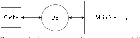
Block diagram of the proposed FFT/IFFT processor is
depicted in Fig. 4. It consists of four FFT/IFFT control units, a
main memory unit, a processing engine (PE), and a 64-word
cache. In this design, a novel block scaling method and a new
ping-pong cache-memory architecture are proposed to reduce
the power consumption and hardware cost. Besides, since
FFT and IFFT have the same operations except for complex-
conjugated twiddle factors, we implement IFFT by simply
taking conjugates of FFT input/output [6] as shown in Fig. 4.
With these techniques and proper data scheduling, the
proposed design can realize two 2048-point FFT/IFFT
computations in 2052 clock cycles. Thus by taking the guard
interval of WiMAX systems into account, the proposed
FFT/IFFT processor does not need to operate in a multiple
sampling frequency as the previous cached-memory FFT
designs do [2], [3]. The modules of the proposed design will
be described in more detail below.
Fig. 4. Block diagram of the proposed two-stream FFT/IFFT processor.
204

A. Main Memory
For memory-based FFT processors supporting consecutive
I/O, multiple main memories are needed as computation and
I/O buffers [7]. To reduce the total memory size, the
continuous flow (CF) memory architecture is proposed [7]
where only two N-word memories are required for N-point
FFT. Although CF FFT can reduce memory size by doing I/O
operation concurrently in a single memory, it requires
additional controls for memory addressing and butterfly units
(BU). This is because the original CF FFT adopts radix-4 and
radix-2 algorithms which have different bit-reverse orders. In
our proposed design; however, CF memory architecture
causes no problem since radix-2
3
and radix-2
2
algorithms
have the same bit-reverse order as radix-2 algorithm [4]. As
shown in Fig. 4, one 4096-word SRAM works as the I/O
buffer while the other one works as the processing buffer, and
vice versa. Each SRAM is further partitioned to eight banks to
support eight accesses simultaneously for radix-2
3
algorithms.
B. Ping-Pong Cache-Memory Architecture
Cached-memory FFT [2], [3] is proposed for low power
consumption by reducing the memory accesses. As shown in
Fig. 5, data are first read from main memory and then sent to
the cache. By proper data scheduling, PE can perform
multiple-stage processing by accessing local cache instead of
the main memory. Although cached-memory FFT can reduce
memory accesses effectively, a concurrent read/write cache
with complex control is required to increase the throughput.
Thus we propose the ping-pong cache-memory architecture
which uses a simple cache with single read/write operations.
As illustrated in Fig. 6, data read from the main memory are
processed by PE first and then written to the cache for future
use. After the cache is full, data in the cache are read by PE
and the computed results are stored back to the main memory.
Since radix-2
3
algorithm is adopted in the proposed design, a
64-word cache is employed to support two-stage radix-2
3
processing. By using this scheme, half the memory accesses
can be saved. Moreover, the ping-pong cache-memory has
shorter latency compared to the cached-memory, which is
beneficial in scheduling data streams.
Fig. 5. Cached-memory architecture.
Fig. 6. Proposed ping-pong cache-memory architecture.
C. Processing Engine (PE)
The PE is designed to perform radix-2
3
/2
2
/2 butterfly
operations and complex multiplications with proposed block
scaling approach as shown in Fig. 7. Since variable-length
FFT must be supported and the final stage can be radix-2
3
,
radix-2
2
, or radix-2 as described earlier, a configurable
radix-2
3
/2
2
/2 butterfly unit capable of processing one radix-2
3
,
two radix-2
2
, or four radix-2 is adopted. We use 2048-point
FFT mode to describe the control of PE. At the fist processing
stage, since the inputs have the same decimal point, data
alignments are skipped. Input data are processed by radix-2
3
BU directly and then passed to the first overflow detection
and scaling unit (ODSU1) in Fig. 7. If an overflow is detected,
all eight inputs will be scaled and the corresponding shift in
exponent is sent to the block scaling unit. Afterward, the
output of ODSU1 is sent to the complex multipliers for
twiddle factor multiplications. The outputs of the complex
multipliers are passed to the second overflow detection and
scaling unit (ODSU2) in Fig. 7 where the same operation of
ODSU1 is performed. The second and third stages have
similar control flows as stage 1. For stage 4, after inputs are
aligned in decimal point for processing, two radix-2
2
operations are performed. At this stage; however, only scaling
is performed in ODSU1 since the final output is
fixed-exponent in our proposed block scaling algorithm.
Complex multiplications and ODSU2 are also skipped in this
stage because no twiddle factor multiplication is required at
final stage as shown previously in Fig. 2. The detailed control
flow for all 128~2048 FFT modes is summarized in Table I.
Fig. 7. Block diagram of the processing engine.
TABLE I. PE control for 128~2048-point FFT/IFFT.
First
Stage
Intermediate
Stage(s)
Final
Stage
Alignment Bypass ON ON
Configurable
BU
Radix-2
3
Radix-2
3
Radix-2
3
for 512 FFT
Radix-2
2
for 256/2048 FFT
Radix-2 for 128/1024 FFT
ODSU1
Detection
& Scaling
Detection
& Scaling
Scaling
Multiplier ON ON Bypass
ODSU2
Detection
& Scaling
Detection
& Scaling
Bypass
Block
scaling
unit
Exponent
store
Alignment
control &
Exponent
store
Alignment
control &
ODSU1
control
IV. C
HIP IMPLEMENTATION
A test chip of the proposed block scaling FFT/IFFT
processor (2048-point mode) is implemented using UMC
0.13 μm 1P8M CMOS technology for verification. The core
size is 1332×1590 μm
2
as shown in Fig. 8. From post-layout
prime power simulation, it is shown that the proposed
205

FFT/IFFT consumes only 17.26 mW at 22.86 MHz when
performing two 2048-point FFT computations consecutively
for WiMAX applications. The SQNR performance of the
2048-point FFT/IFFT has also been verified to exceed 48 dB
for QPSK and 16/64-QAM signals. Thus the implementation
loss of cascaded IFFT and FFT is only 0.1 dB with AWGN at
30 dB SNR which satisfies our design target for WiMAX
applications. The detailed power profiling and chip summary
are shown in Fig. 9.
4096-word SRAM
4096-word SRAM
BSU
ROM
Cache
Cache
BU M7
M1 M2
M3 M4
M6M5
Controller
Fig. 8. Chip layout of the proposed FFT/IFFT Processor.
Fig. 9. Power profiling and chip summary of the proposed processor.
V. C
OMPARISON
For comparisons, we choose two FFT processor chips
which can handle consecutive 2048-point FFT computations
[8], [9]. Since these two chips can not support multiple data
streams and only complete results for 1024-point FFT are
listed, the comparisons of execution time and power are based
on single-stream 1024-point FFT. Besides, to compare the
FFT processor chips fabricated with different technologies,
we adopt the normalized area and FFTs per energy [2] as our
performance indices shown in eqs. (3) and (4). Note that eq.
(4) has been adapted to take account of the voltage scaling.
2
Area
Normalized Area
(Technology/0.13μm)
=
(3)
2
3
(Technology/0.13μm) ( /1.2)
FFTs
Normalized
Energy Power Execution Time 10
DD
V×
=
××
(4)
The comparison results are summarized in TABLE II. We
can find that the FFT processor [9] use a shorter wordlength
of 12 bits since it only supports for 9-bit input. The processor
[8] has employed the BFP approach and thus the wordlength
is not increased. However, both designs [8], [9] do not employ
a cache design to reduce the power of memory accesses. From
this comparison, it is shown that our proposal has a
satisfactory result in both normalized area and FFTs per
energy, which justifies the feasibility of the proposed method.
TABLE II. Chip comparison of various 2048-point FFT Processors.
This Work Zhong [8] Lin [9]
*3
Technology 0.13 μm 0.25 μm 0.35 μm
Supported FFT/
IFFT (consecutive)
Two 2048-point
*1
FFTs/IFFTs
8~2048-point
FFT
512~2048-point
FFT
Cache design Yes No No
Scaling/BFP design Block scaling BFP No
Input bit width 12 bits 16 bits 9 bits
Wordlength 12 bits 16 bits 12 bits
Core voltage 1.2 volt 2.5 volt 3.3 volt
Clock rate 22.86 MHz 200 MHz 45.45 MHz
Execution time
(1024-point)
22.48 μs
*2
26.4 μs 45.06 μs
Power (1024-point) 17.26 mW
*2
400 mW 640 mW
Core Area
2.12 μm
2
11.42 μm
2
13.05 μm
2
Normalized 1024-
Point FFTs/ Energy
2577
*2
790 706
Normalized Area 1.06 3.09 1.80
*1: Can be extended to 128~2048-point by adding control modes.
*2: Normalized from data of two 2048-point FFTs.
*3: The bit-reverse memory is not included.
VI. C
ONCLUSION
A block scaling MIMO FFT/IFFT processor for WiMAX
applications has been proposed in this paper. It can support
two 2048-point FFT/IFFT computations simultaneously
within 2052 clock cycles. Moreover, with a novel block
scaling method and a new ping-pong cache-memory
architecture, both power consumption and hardware cost can
be greatly reduced. A test chip has been designed using UMC
0.13 μm 1P8M process. Simulation result has shown that the
proposed FFT processor consumes only 17.26 mW at 22.86
MHz which meets the maximum throughput rate of WiMAX
applications.
A
CKNOWLEDGMENT
This work was supported by the National Science Council
of Taiwan under Grant NSC94-2215-E-009-044 and
by ICL/ITRI. under Grant 5352BA5115.
REFERENCES
[1] WiMAX Forum, Mobile WiMAX-Part I: A technical overview and
performance evaluations, Feb. 21, 2006.
[2] B. M. Bass, “A low-power, high-performance, 1024-point FFT
processor,” IEEE J. Solid-State Circuits, vol. 34, pp. 380–387, Mar.
1999.
[3] Y.-W. Lin, H.-Y. Liu, and C.-Y. Lee, “A dynamic scaling FFT
processor for DVB-T applications,” IEEE J. Solid-State Circuits, vol.
39, pp. 2005–2013, Nov. 2004.
[4] He Shousheng and M. Torkelson, “Designing pipeline FFT processor
for OFDM (de)modulation,” In Proc. Int. Symp. Signals, Systems,
and Electronics, 29 Sept.-2 Oct. 1998, pp. 257-262.
[5] B. M. Baas, “An approach to low-power, high-performance, fast
Fourier transform processor design,” PhD Dissertation, Stanford
University, Stanford, CA, 1999.
[6] K. Maharatna, E. Grass, and U. Jagdhold, “A 64-point Fourier
transform chip for high-speed wireless LAN application using
OFDM,” IEEE J. Solid-State Circuits, vol. 39, pp. 484-493, Mar.
2003.
[7] B. G. Jo and M. H. Sunwoo, “New continuous-flow mixed radix
(CFMR) FFT using novel in-place strategy,” IEEE Trans. Circuits
Syst., vol. 52, pp. 911–919, May. 2005.
[8] G. Zhong, F. Xu, and A. N. Willson Jr., “A power-scalable
reconfigurable FFT/IFFT IC based on a multi-processor ring,” IEEE
J. Solid-State Circuits, vol. 41, pp. 483-495, Feb. 2006.
[9] Y.-T. Lin, P.-Y. Tsai, and T.-D. Chiueh, “Low-power variable-
length fast Fourier transform processor,” In Proc. Comput. Digit.
Tech., vol. 152, No. 4, pp. 499-506, July 2005.
206