scispace - formally typeset
Open AccessJournal ArticleDOI

An updated roadmap for the integration of metal–organic frameworks with electronic devices and chemical sensors

Reads0
Chats0
TLDR
This review highlights the research aimed at the implementation of MOFs as an integral part of solid-state microelectronics and discusses the fundamental and applied aspects of this two-pronged approach.
Abstract
Metal-organic frameworks (MOFs) are typically highlighted for their potential application in gas storage, separations and catalysis. In contrast, the unique prospects these porous and crystalline materials offer for application in electronic devices, although actively developed, are often underexposed. This review highlights the research aimed at the implementation of MOFs as an integral part of solid-state microelectronics. Manufacturing these devices will critically depend on the compatibility of MOFs with existing fabrication protocols and predominant standards. Therefore, it is important to focus in parallel on a fundamental understanding of the distinguishing properties of MOFs and eliminating fabrication-related obstacles for integration. The latter implies a shift from the microcrystalline powder synthesis in chemistry labs, towards film deposition and processing in a cleanroom environment. Both the fundamental and applied aspects of this two-pronged approach are discussed. Critical directions for future research are proposed in an updated high-level roadmap to stimulate the next steps towards MOF-based microelectronics within the community.

read more

Content maybe subject to copyright    Report

An updated roadmap for the integration of metal–organic
frameworks with electronic devices and chemical sensors
Ivo Stassen,
ab
Nicholas Burtch,
c
Alec Talin,
c
Paolo Falcaro,
de
Mark Allendorf
c
and Rob Ameloot *
a
Metal–organic frameworks (MOFs) are typically highlighted for their potential application in gas storage, separations and catalysis. In
contrast, the unique prospects these porous and crystalline materials offer for application in electronic devices, although actively
developed, are often underexposed. This review highlights the research aimed at the implementation of MOFs as an integral
part of solid-state microelectronics. Manufacturing these devices will critically depend on the compatibility of MOFs with existing
fabrication protocols and predominant standards. Therefore, it is important to focus in parallel on a fundamental understanding of the
distinguishing properties of MOFs and eliminating fabrication-related obstacles for integration. The latter implies a shift from the
microcrystalline powder synthesis in chemistry labs, towards film deposition and processing in a cleanroom environment. Both
the fundamental and applied aspects of this two-pronged approach are discussed. Critical directions for future research are
proposed in an updated high-level roadmap to stimulate the next steps towards MOF-based microelectronics within the community.
1. Introduction
The structure and dynamics of matter at the nanometer scale
form the basis for both natural processes and technological
applications. For instance, ions moving across a lipid membrane
and in between electrodes are essential to living cells and
batteries, respectively. Similarly, our sense of smell and detectors
for hazardous substances are both based on the recognition of
a
Centre for Surface Chemistry and Catalysis, KU Leuven University of Leuven,
Celestijnenlaan 200F, B-3001 Leuven, Belgium. E-mail: rob.ameloot@ku leuven.be
b
Imec, Kapeldreef 75, B-3001 Leuven, Belgium
c
Sandia National Laboratories, Livermore, CA 94551-0969, USA
d
Institute of Physical and Theoretical Chemistry, Graz University of Technology,
Stremayrgasse 9, 8010 Graz, Austria
e
Department of Chemistry, The University of Adelaide, Adelaide, South Australia
5005, Australia
Ivo Stassen
Ivo Stassen is a Postdoctoral
Fellow of the Research
Foundation Flanders (FWO)
working at the University of Leu-
ven and Imec. He received his
MSc in Bioscience Engineering at
KU Leuven in 2012, followed by a
PhD in 2016. In 2014–2015, he
worked a as visiting scholar at
Kyoto University. His research
interests include solvent-free and
gas-phase synthesis of metal–
organic frameworks, host–guest
properties and fabrication of
functional nanoporous structures such as thin films, patterns and
devices.
Nicholas Burtch
Nicholas Burtch is a Harry S.
Truman Fellow at Sandia National
Laboratories in Livermore, CA. He
received his BSE from the University
of Michigan and PhD fro m the
Georgia Institute of Technology,
both in chemical engineering. His
research interests include the
experimental synthesis and
computational understanding of
crystalline, nanoporous materials
for materials science and
adsorption applications.

small molecules. To optimize interactions and processes at this
length scale, one would ideally be able to structure matter at the
(sub-)nanometer level. Indeed, in living organisms, precisely
tuned nano-environments are provided by ion channels and
dedicated receptors that are formed through self-assembly of
molecular building blocks. Man-made devices, on the other
hand, typically rely on much cruder fabrication tools: even
cutting-edge lithographic techniques fall at least an order of
magnitude short in resolution to structure matter at the desired
length scale.
Nevertheless, precisely controlled nano-environments do
exist in synthetic materials. Metal–organic frameworks (MOFs)
are crystalline nanoporous materials built out of metal-based
nodes and multitopic organic ligands (also called linkers)
connected by coordination bonds (Fig. 1a).
1
Over the last two
decades, MOFs have grown into promising materials for a wide
range of potential applications in industry and society. The
chemistry of these materials is characterized by the features of
their high-surface area crystal lattices: short and long range
ordering, intrinsic nanoporosity with pores of tunable size,
versatile host–guest chemistries (‘‘guest@MOF’’ properties)
and responsiveness to physical and chemical stimuli. What is
more, the synthetic chemistry that enables these features is
based on the spontaneous self-assembly of simple molecular
building units, which permits the ‘‘design’’ of MOF lattices
based on linkers and nodes with known geometries and
coordination environments. Hence, MOFs as a high-surface
area material platform, at the interface between hard and soft,
Alec Talin
Alec Talin has been a member of
the technical staff at Sandia
National Laboratories since 2002.
He is also an adjunct associate
professor of materials science and
engineering at the University of
Maryland. He received a BA
degree in chemistry from the
University of California, San
Diego in 1989, and a PhD
degree in materials science and
engineering from the University of
California, Los Angeles, in 1995.
Prior to joining Sandia, he spent
six years at Motorola Labs, and was a project leader at the Center
for Nanoscale Science and Technology at the National Institute of
Standards and Technology. His research focuses on areas of novel
electronic materials, energy storage and conversion, and national
security. He is a principal editor of the journal MRS Communications.
Paolo Falcaro
Paolo Falcaro is professor in
Biobased Materials and Techno-
logies at Graz University of
Technology (TU Graz Graz, Aus-
tria). He received his PhD in mate-
rials engineering in 2006 from
Bologna University, Italy. From
2005 to 2009 he worked at
Civen/Nanofab (Venice, Italy) as
manager of the sol–gel technology
for industrial applications. In
2009 he joined CSIRO (Mel-
bourne, Australia), extending the
expertise from sol–gel and device
fabrication to metal–organic frameworks. In 2011 he received the
ARC DECRA, progressing from group leader to team leader in 2014.
In 2016 he joined the Institute of Physical and Theoretical Chemistry
at TU Graz.
Mark Allendorf
Mark Allendorf is Director of
theHydrogenAdvancedMaterials
Research Consortium and a senior
scientist at Sandia National Labora-
tories. He received an AB degree
in chemistry from Washington
University in St. Louis and a PhD
degree in chemistry from Stanford
University. His research focuses on
the fundamental science and
applications of metal–organic fra-
meworks and related materials. He
has been published in more than
160 publications, including more
than 120 journal articles. He is President Emeritus and Fellow of The
Electrochemical Society and his awards include a 2014 R&D 100 Award
for a novel approach to radiation detection.
Rob Ameloot
Rob Ameloot obtained his PhD in
Bioscience Engineering/Catalytic
Technology at KU Leuven
(Belgium) in 2011. In 2012–
2013, he worked with Jeffrey Long
as a Fulbright postdoctoral fellow
at UC Berkeley (US). Currently,
he is a tenure-track research
professor at the KU Leuven
Centre for Surface Chemistry
and Catalysis. He was awarded
an ERC starting grant to work on
bringing metal–organic frame-
works from the chemistry lab into
the microelectronics fab by developing vapor phase thin film
deposition routes. In general, he is passionate about pushing the
envelope in porous materials and process technology, with a
healthy disregard for traditional subject boundaries.

inorganic and organic materials, offer a new window for fine-
tuning various structure–property relationships.
MOFs are typically obtained as microcrystalline powders
through solvothermal synthesis. Therefore, MOF research initially
focused on evaluating and optimizing the physical and chemical
properties in the context of bulk applications: gas storage and
chemical engineering operations (catalysis, separation).
2,3
These
fields build on the prior research and industrial implementation
of related materials, e.g. nanoporous silicates such as zeolites.
More recently, the unique properties of MOFs encouraged
research lines atypical for porous materials, often in areas
where the introduction of ordered porosity promises new
concepts entirely. In contrast to the proposed bulk applications
of MOFs, these more recent directions frequently target high-
value technological areas requiring very little material in
comparison. Examples include MOFs as functional materials
in chemical analytics, biomedical technology, solid-state
material physics and various other branches of nanoscience
and technology.
4
This review highlights the research aimed at the implemen-
tation of MOFs as an integral part of solid-state devices. In this
context, ‘‘integration’’ denotes that the MOF is an integral
component of the actual device structure and that the
fundamental aspects of device or circuit design are being taken
into account at least rudimentarily. We focus in particular on
electronic devices, which broadly defined are physical entities
that influence electrons when connected to an electrical circuit.
Examples of electronic devices include individual components
such as resistors, transistors and diodes, as well as assemblies
of such components such as amplifiers, sensors and micro-
controllers. Our everyday life increasingly relies on ever more
capable electronic devices including smartphones and computer
processors based on millions of miniaturized logic units, mem-
ory arrays and input/output interfaces such as physical sensors,
actuators and displays. The enormous success of electronic
devices has mainly been enabled by low-cost production through
scalable ‘‘CMOS’’ microfabrication (CMOS = complementary
metal-oxide–semiconductor). The renowned ‘‘Moore’s law’’ stat-
ing that the number of transistors in integrated circuits doubles
every two years, has been a self-imposed driving force for CMOS
research and downsizing in academia and industry since the
1970s. Importantly, this downsizing course has not only been
enabled by improved fabrication tools, but to an equal extent by
advances in materials science that ensure reliable performance
of ever tinier circuit elements. Industrial and academic research
efforts in this context have for long been harmonized by the
Fig. 1 Graphical representation of MOF, their structural and chemical versatility and some representative concepts related to device applications.
(a) MOFs are ordered frameworks built from interconnected organic ligands and metal-based nodes. The broad-scope recommended definition of a
MOF: ‘‘Coordination network with organic ligands containing potential voids; coordination network being a coordination compounds extending in at
least one dimension through repeating coordination entities’’.
6
(b) Some key properties of MOFs that may lead to applications in electronic devices.
(c) The burgeoning field of MOF devices visualized through the seminal example of chemical sensors. Shown is the evolution of the yearly publications
that combine the concepts ‘‘metal–organic framework’’ and ‘‘sensor’’ (source: SciFinder
s
). The earliest demonstrations of some general concepts, as
well as the 2011 roadmap article (no. 1), are positioned on the same timeline.

International Technology Roadmap for Semiconductors (ITRS).
These reports composed by semiconductor industry experts
specify research directions and targets in order to meet needed
material, fabrication and device specifications. In 2011, these
guidelines inspired some of us to stipulate a first roadmap for
exploratory research on MOFs in electronics.
5
Today, circa five
years of research later, this review provides an updated overview.
Analogous to the previous paper, progress in different areas of
interest is reviewed and perspectives and suggested focus points
are stipulated. Although arguably arbitrary, we strictly limit this
discussion to MOFs and exclude most of the larger family of
coordination polymers, most of which are nonporous.
6
One of the key trends in microelectronics is a gradual shift
from inorganic and silicon-centered, towards organic and
hybrid organic–inorganic devices. Depending on the applica-
tion scenario, this route is followed either to benefit from the
greater compositional complexity of organics, to reduce
production costs, or to push downsizing to the limit, down to
molecular dimensions. In the context of digital logic, such
approaches are referred to as ‘‘beyond CMOS’’, as CMOS-based
scaling in silicon technology will run into fundamental limita-
tions. Technologies based on new materials such as graphene
promise scaling beyond the limitations of silicon and are on the
verge of causing paradigm shifts in several areas.
7
Application
areas in which similar transitions are either impending or
already commercially implemented include photovoltaic cells
(cf. from silicon to perovskite or dye-sensitized solar cells) and
displays (cf. from indium tin oxide to polymers). This shift in
materials scope is accompanied by a rising interest in molecular
approaches and a rising acceptance and economic viability of
alternative manufacturing approaches such as inkjet printing
and roll-to-roll manufacturing. In our opinion, the continuous
exploration of new materials and properties combined with an
increasing attention for bottom-up strategies at a length scale
where chemistry and materials science merge could make elec-
tronic devices one of the most interesting proving grounds
for MOFs.
Directly related to their structure, MOFs offer properties
outside the existing materials scope in electronics: e.g. sensor
coatings with adsorption properties geared to specific analytes,
dielectric properties tunable at will, intrinsic porosity that
allows through-solid mass and ion transport, mechanical proper-
ties in between polymers and inorganics and electronic conduc-
tance tunable from practically zero to over a hundred S cm
2
(Fig. 1b). Within this range of potential applications, chemical
sensing seems to be the first to shift from proof of concept to the
development stage, arguably due to the directly transferable
adsorption studies available from researching bulk applications.
Nevertheless, recent milestones such as the design and synthesis
of a first generation of highly conductive MOFs (2014–2015) and
the fabrication of a field effect transistor, FET, (2016) highlight
the potential of MOFs in future electronic devices (Fig. 1c). The
primary prerequisite for realizing such MOF-based devices is a
radical performance increase over established technologies.
Moreover, manufacturing these devices will critically depend
on the compatibility of MOFs with existing fabrication protocols
and predominant standards. Therefore, it is important that
research efforts focus in parallel on a fundamental understand-
ing of the distinguishing properties of MOFs and eliminating
fabrication-related obstacles for integration. For MOFs, the latter
implies a shift from the microcrystalline powder synthesis in
chemistry labs, towards film deposition and processing in a
cleanroom environment. Moreover, it is important that the field
moves beyond the synthetic and structural aspects to engage
experts in other fields, such as materials science, physics, and
electrical engineering and to realize the use of MOFs in devices.
In this review, both aspects of the two-pronged approach
suggested above are highlighted. Progress in understanding
relevant fundamental physical properties of MOFs is discussed
first. Secondly, the general context of device microfabrication is
outlined and relevant MOF research is put in perspective.
Thirdly, case studies of MOF integration in electronic devices
are discussed for different application fields. Lastly, general
progress of the field, outstanding obstacles and perspectives
are outlined.
2. Fundamental MOF properties
A crucial requirement for designing and fabricating electronic
devices incorporating MOFs is knowledge of their basic charge
transport, photonic, and magnetic properties. Compared to
established materials such as silicon and organic semiconduc-
tors, little is known about MOFs. However, considerable pro-
gress has been made since the original 2011 roadmap,
5
providing ample reason to envision that MOFs could have a
prominent place in future electronic devices. Several review
articles already provide in-depth summaries of various aspects
of MOF research that are relevant to electronic applications.
Our intention here is not to exhaustively cover the same
ground, but rather to discuss recent milestones that highlight
progress and to identify opportunities and critical needs for
advancing the field. Relevant review articles for further reading
will be cited where applicable. Following the structure of the
first-generation roadmap, in this section we update the status
of charge transport, optical, and light generation. New sections
concerning magnetic properties and light harvesting are also
included.
2.1 Electronic conductivity
The ability to conduct electrical charge is perhaps the most
important and also least explored property of MOFs to devel-
oping them as active materials in electronic devices. Most
MOFs are electrical insulators, but in the last five years this
subcategory has expanded from merely two structures in 2011
to about two dozen materials with demonstrated conductivity
or charge mobility. This ten-fold increase motivated a recent
review article by Dinca
˘
and coworkers that identifies strategies
for designing electronically conducting MOFs.
8
These results,
although limited, are nevertheless highly encouraging. How-
ever, the best MOF conductivities obtained so far are still low by
comparison with other types of conducting materials (Table 1).

Although nonporous coordination polymers such as poly(Ni
1,1,2,2-ethenetetrathiolate), a rare example of a hybrid n-type
semiconductor, are certainly of interest, we confine the discus-
sion here to conducting MOFs that are clearly nanoporous. The
next two sections provide first a brief introduction to charge
transport from a solid-state physics point of view and its
connection with MOFs, then a summary of charge transport
mechanisms known to be operative in MOFs.
Fundamentals of charge transport. According to band theory,
solids can be classified as insulators, semiconductors, or metals
based on the magnitude of the energy gap, E
g
,separatingthe
valence band (VB) from the conduction band (CB): E
g
4 4eVare
insulators, 0 o E
g
o 3 eV are semiconductors, and E
g
o 0
(i.e. partially filled band) are metals.
9
The band model works well
for many solids in which strong electronic coupling between
neighboring atoms leads to large band dispersion (i.e. large DE
between bonding and antibonding orbitals) that makes it ener-
getically favorable to delocalize carriers across many lattice sites.
For solids with large band dispersion (also known as ‘‘band-
width’’) such as Si (Fig. 2a), the energy gained by delocalizing the
charge (BW/2) makes the electron–electron repulsion effects
insignificant. In metals, the repulsion effects relative to Si are
further reduced electrostatically by the large density of free
carriers. However, true metallic conduction (i.e. decreasing con-
ductivity with increasing temperature) is not observed in many
materials with bandwidth less than B0.5 eV. This is the case
even when the Fermi level moves into the VB or the CB due to
strong carrier localization; here, the carriers are energetically
Table 1 Comparison of conductivity data for a selection of MOFs and other conducting materials
Material or formula unit Conductivity (S cm
1
) Charge carrier
e
Mobility (cm
2
V
1
s
1
) Ref.
Copper 10
5
–10
6
e46 41
Doped polyacetylene 560 (n); 360 (p) h or e 1 (n-doped, cis)42
Undoped polyacetylene 10
9
42
Doped polyaniline 10
3
41
Graphene 550
b
41
Polycrystalline graphite 1250 43
Polythiophenes 1975 h 1–10 29 and 44
Rubrene 445
TTF-TCNQ 700 41
Cu[Ni(PDT)
2
](I
2
doped) 1 10
4 a
12
Cu
3
(BHT)
2
d
1580
b
h or e 99 (h); 116 (e) 46
Ni
3
(HITP)
2
2;
a
40
b
h or e 48.6 28 and 31
Ni
3
(BHT)
2
0.15;
a
2.8–160
c
47 and 48
Mn
2
(DOBDC) 3.9 10
13 a
49
Fe
2
(DOBDC) 3.2 10
7 a
49
Mn
2
(DSBDC) 1.2 10
12 a
0.01 49 and 50
{[Cd
2
(AZBPY)
2
(HO-1,3-BDC)
2
](AZBPY)(H
2
O)}
n
1.86
b
e51
K
1.2
Ru
3.6
[Ru(CN)
6
]
3
16H
2
O 5.7 10
3
36
TCNQ@Cu
3
(BTC)
2
0.07
b
h18
TCNQ@[Cu(TPyP)Cu
2
(O
2
CCH
3
)
4
] 2.5 10
6
34
Zn
2
(TTFTB) 4.0 10
6
0.2 22
Porphyrin Zn-SURMOF-2 h 0.002 52
Pd@porphyrin Zn-SURMOF-2 h 0.003–0.004 52
[Sr(HBTC)(H
2
O)]
n
10
9
–10
7 a
32
NNU-7 (anthracene MOF) 1.3 10
3 c
24
(NBu
4
)
2
Fe
2
(DHBQ)
3
0.16
a
15
Sample morphologies used for conductivity measurements, if specified:
a
pellet;
b
film;
c
microflakes or single crystal.
d
Coordination polymer
without any indication of guest-accessible porosity.
e
h: hole; e: electron.
Fig. 2 Calculated band diagrams. (a) Si. Adapted from ref. 9. Copyright 2011 Springer. (b) MOF-5. Reproduced with permission from ref. 10.
(c) Ni
3
(HITP)
2
. Reproduced with permission from ref. 14. Copyright 2016 American Chemical Society. The band width (W) is approximately 8 eV, 0 eV,
and 0.8 eV, respectively.

Figures
Citations
More filters
Journal ArticleDOI

Reversible Optical Writing and Data Storage in an Anthracene‐Loaded Metal‐Organic Framework

TL;DR: This work shows how the confinement of anthracene in a well-chosen MOF host leads to reversible yellow-to-purple photoswitching of the fluorescence emission, which holds promise in product authentication and secure communication applications.
Journal ArticleDOI

Dual-emissive ratiometric fluorescent probe based on Eu3+/C-dots@MOF hybrids for the biomarker diaminotoluene sensing

TL;DR: In this article, a ratiometric fluorescence hybrid probe Eu3+/C-dots@MIL-53 (1a) has been synthesized by encapsulating the luminescent carbon dots and lanthanide ions into the metal-organic framework to yield the dual-emitting composite.
Journal ArticleDOI

Rare earth metal–organic frameworks (RE-MOFs): Synthesis, properties, and biomedical applications

TL;DR: The potential utility of rare earth metal-organic frameworks has been explored with particular emphasis on drug delivery, fluorescent/magnetic resonance imaging, and biomedical sensing fields based on a comparative evaluation of the related literature.
Journal ArticleDOI

Epitaxial Growth and Integration of Insulating Metal–Organic Frameworks in Electrochemistry

TL;DR: This work introduces an epitaxial growth strategy to accomplish the efficient integration of the insulating MOFs into electrochemistry and sheds light on integrating insulate MOF/graphene 2D architecture.
References
More filters
Journal ArticleDOI

The Chemistry and Applications of Metal-Organic Frameworks

TL;DR: Metal-organic frameworks are porous materials that have potential for applications such as gas storage and separation, as well as catalysis, and methods are being developed for making nanocrystals and supercrystals of MOFs for their incorporation into devices.
Journal ArticleDOI

Functional porous coordination polymers.

TL;DR: The aim is to present the state of the art chemistry and physics of and in the micropores of porous coordination polymers, and the next generation of porous functions based on dynamic crystal transformations caused by guest molecules or physical stimuli.
Journal ArticleDOI

The missing memristor found

TL;DR: It is shown, using a simple analytical example, that memristance arises naturally in nanoscale systems in which solid-state electronic and ionic transport are coupled under an external bias voltage.
Journal ArticleDOI

Verwendung von Schwingquarzen zur Wägung dünner Schichten und zur Mikrowägung

TL;DR: In this paper, eigenfrequenz der Platte infolge Vergroserung der schwingenden Masse is vermessen, so das eine empirische Eichung bei der Schichtwagung mit Schwingquarzen entfallt.
Related Papers (5)
Frequently Asked Questions (18)
Q1. What is the method for forming a free-standing MOF film?

The solvent–air interface or the boundary layer between immiscible solvents can be used to grow a free-standing MOF film that can be subsequently transferred to a substrate. 

This review highlights the research aimed at the implementation of MOFs as an integral part of solid-state microelectronics. Both the fundamental and applied aspects of this two-pronged approach are discussed. 

A low density of electrically active defects and high charge mobility are also essential for an efficient LED so that injected holes and electrons can penetrate the emitting layer(s) and recombine to form excitons withminimal non-radiative recombination. 

MOFs are well suited to serve as the dye (i.e. light harvesting) component of a DSSC by virtue of the ability to build structures with multiple light absorbers locked into a stable crystalline structure. 

The same material characteristics that make MOFs attractive for charge transport operate here, namely synthetic tunability, long-range order and porosity as an additional design element. 

In AC circuit analysis, the generalized concept of impedance (Z, O) is defined in analogy to DC resistance, as the voltage to current ratio. 

in some cases the MOF phase has an intrinsic preference for alignment parallel to the surface, because of the formation of well-defined crystal faces or the inherently layered nature of the material. 

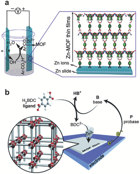
For instance, in a synthesis solution containing Zn(II) nitrate and terephthalic acid, the generation of OH ions through reduction of the NO3anion results in ligand deprotonation and formation of a MOF-5 film on the cathode. 

The approach of using metal oxide films as precursors for MOF coatings benefits from a range of established technologies for deposition of the former (PVD, CVD, ALD, sol–gel methods, etc.). 

While most of the proton-conducting frameworks require hydration, several promising strategies have been developed for anhydrous proton transport in MOFs. 

replacing these systems with solid-state electrolytes is an active research topic, mainly because of their volatility, flammability and reactivity towards the electrodes. 

In the context of microelectronic devices, integration of liquid components as part of vertical stacks is not possible due to structural reasons and incompatibility with vacuum technology. 

Although nano-indentation is becoming a more common tool to characterize single MOF crystals and thin film, few materials have been characterized in depth. 

To fabricate the first FETs based on semiconducting MOFs,28,46 interfacial growth processes were combined with subsequent film transfer. 

Compared to established thin film deposition technologies (e.g. sol–gel methods, PVD, CVD, ALD), MOF films typically show a higher roughness, often above 10% of the film thickness. 

In contrast to purely inorganic or organic conductors such as MoS2 or graphene, which do not easily lend themselves to chemical functionalization, the electronic properties of MOFs can be tuned by chemically altering the linker, metal ion or guest species adsorbed in the pore space. 

recent studies demonstrated that analyte-permeable dielectric sensing materials can also be screened using the KP method. 

It will be interesting to see the performance gain by combining MOFs with more recent sensors that exploit different elastic wave propagation modes including acoustic-plate-mode and flexural-plate-wave devices.