scispace - formally typeset
Open AccessJournal ArticleDOI

A comprehensive model of PMOS NBTI degradation

Reads0
Chats0
TLDR
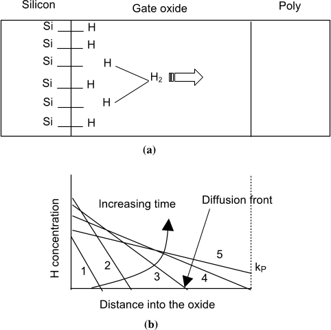
A comprehensive model for NBTI phenomena within the framework of the standard reaction–diffusion model is constructed and it is demonstrated how to solve the reaction-diffusion equations in a way that emphasizes the physical aspects of the degradation process and allows easy generalization of the existing work.
About
This article is published in Microelectronics Reliability.The article was published on 2005-01-01 and is currently open access. It has received 710 citations till now. The article focuses on the topics: Negative-bias temperature instability.

read more

Figures
Citations
More filters
Proceedings ArticleDOI

Electron trapping: An unexpected mechanism of NBTI and its implications

TL;DR: In this paper, the authors demonstrate that electron trapping has been overlooked in previous studies and will greatly impact the current understanding of the NBTI phenomenon and consequent lifetime predictions and demonstrate that the electron trap has the ability to trap electrons.
Journal ArticleDOI

Negative bias temperature instability modeling for high-voltage oxides at different stress temperatures

TL;DR: An enhanced reaction–diffusion model including trap-controlled transport, the amphoteric nature of the Pb centers at the Si/SiO2 interface, Fermi-level dependent interface charges, and fully self-consistent coupling to the semiconductor device equations is presented.
Proceedings ArticleDOI

BTI-aware design using variable latency units

TL;DR: This work develops variable latency unit (VLU) based BTI-aware designs, with a novel scheme for multioutput hold logic implementation for VLUs, using an adaptive body bias framework to achieve high performance.
Proceedings ArticleDOI

Sensor-wise methodology to face NBTI stress of NoC buffers

TL;DR: This paper presents a novel cooperative sensor-wise methodology to reduce the NBTI degradation in the network on-chip (NoC) virtual channel (VC) buffers, considering process variation effects as well.
Journal ArticleDOI

Bias temperature instability in scaled CMOS technologies: A circuit perspective

TL;DR: The understanding of the BTI mechanism in scaled CMOS technologies is summarized and the correlation between discrete device degradation and circuit/SRAM aging is discussed.
References
More filters
Journal ArticleDOI

Anomalous transit-time dispersion in amorphous solids

TL;DR: In this paper, the authors developed a stochastic transport model for the transient photocurrent, which describes the dynamics of a carrier packet executing a time-dependent random walk in the presence of a field-dependent spatial bias and an absorbing barrier at the sample surface.
Book

The physics of amorphous solids

TL;DR: The formation of amorphous solids Amorphous Morphology: The Geometry and Topology of Disorder Chalcogenide Glasses and Organic Polymers The Percolation Model Localization Delocalization Transitions Optical and Electrical Properties Index as discussed by the authors.
Journal ArticleDOI

Negative bias temperature instability: Road to cross in deep submicron silicon semiconductor manufacturing

TL;DR: The negative bias temperature instability (NBTI) commonly observed in p-channel metaloxide-semiconductor field effect transistors when stressed with negative gate voltages at elevated temperatures is discussed in this article.
Journal ArticleDOI

Negative bias stress of MOS devices at high electric fields and degradation of MNOS devices

TL;DR: A detailed study of the increase of the number of surface traps in MOS structures after NBS at temperatures (25-125°C) and fields (400-700 MV/m) comparable to those used in MNOS devices is presented in this article.
Journal ArticleDOI

Characteristics of the Surface‐State Charge (Qss) of Thermally Oxidized Silicon

TL;DR: In this paper, the surface state charge associated with thermally oxidized silicon has been studied experimentally using MOS structures and the results indicate that the surface-state charge can be reproducibly controlled over a range 1010-1012 cm -2, and it is an intrinsic property of the silicon dioxide-silicon system.
Related Papers (5)
Frequently Asked Questions (2)
Q1. What contributions have the authors mentioned in the paper "A comprehensive model of pmos nbti degradation" ?

In this paper, the authors construct a comprehensive model for NBTI phenomena within the framework of the standard reaction–diffusion model. The authors demonstrate how to solve the reaction–diffusion equations in a way that emphasizes the physical aspects of the degradation process and allows easy generalization of the existing work. The authors also augment this basic reaction–diffusion model by including the temperature and field-dependence of the NBTI phenomena so that reliability projections can be made under arbitrary circuit operating conditions. 

One of the key goal of their future work would be to clarify the role of such processing changes on NBTI performance.